XRT91L32 Просмотр технического описания (PDF) - Exar Corporation
Номер в каталоге
Компоненты Описание
производитель
XRT91L32 Datasheet PDF : 37 Pages
| |||
xr
REV. 1.0.2
XRT91L32
STS-12/STM-4 OR STS-3/STM-1 SONET/SDH TRANSCEIVER
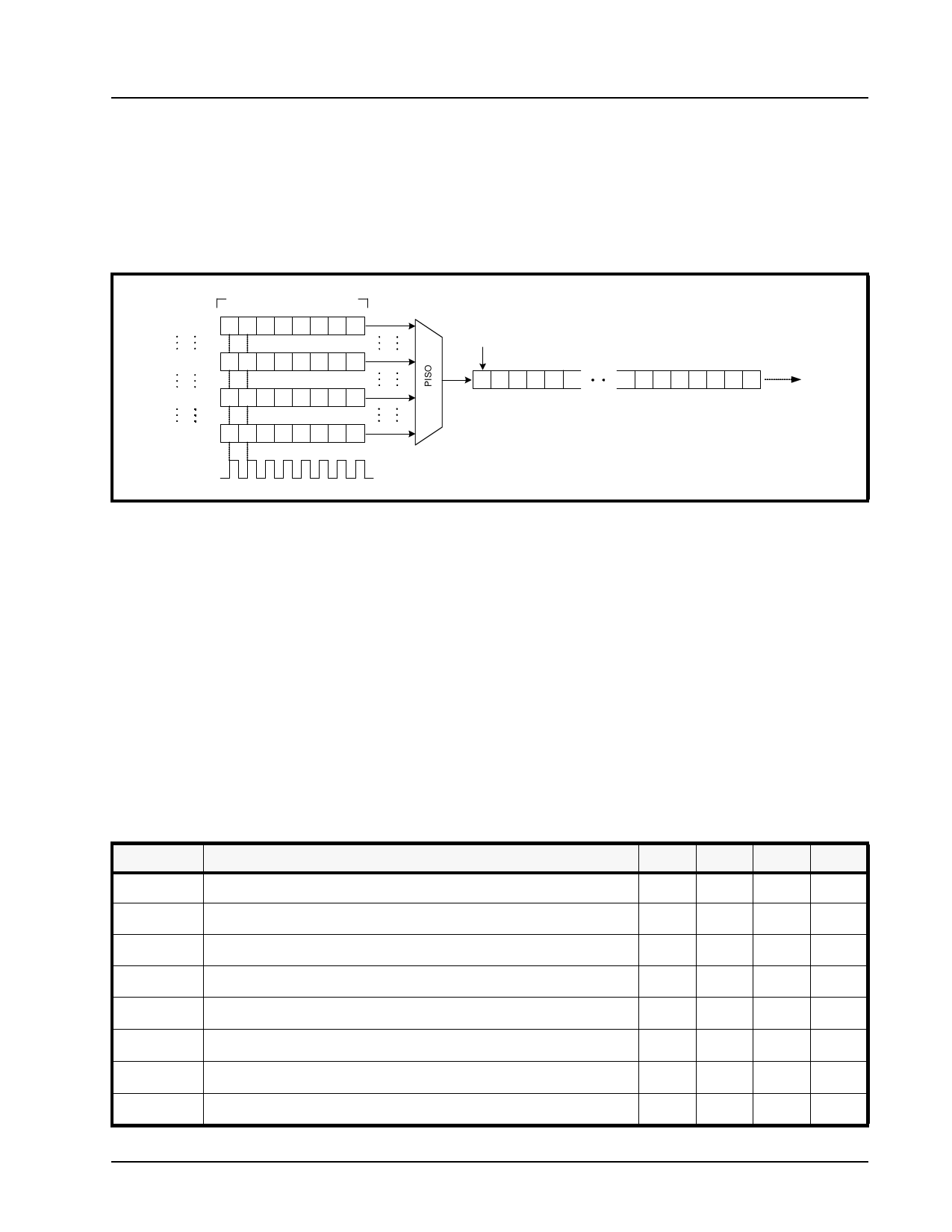
3.3 Transmit Parallel Input to Serial Output (PISO)
The PISO is used to convert 77.76 Mbps or 19.44 Mbps parallel data input to 622.08 Mbps STS-12/STM-1 or
155.52 Mbps STS-3/STM-1 serial data output respectively, which can interface to an optical module. The
PISO bit interleaves parallel data input into a serial bit stream taking the first bit from TXDI7, then the first bit
from TXDI6, and so on as shown in Figure 13.
FIGURE 13. SIMPLIFIED BLOCK DIAGRAM OF PISO
TXDI0
8-bit Parallel LVTTL Input Data
b07 b06 b05 b04 b03 b02 b01 b00
TXDIn
bn7 bn6 bn5 bn4 bn3 bn2 bn1 bn0
TXDIn+
bn+7 bn+6 bn+5 bn+4 bn+3 bn+2 bn+1 bn+0
TXDI7
b77 b76 b75 b74 b73 b72 b71 b70
time (0)
622.08 Mbps STS-12/STM-4 or
155.52 Mbps STS-3/STM-1 serial data rate
b70 b60 b50 b40 b30 b20
b77 b67 b57 b47 b37 b27 b17 b07
TXPCLK_IO
77.76 MHz (STS-12/STM-4) or 19.44 MHz (STS-3/STM-1)
TXOP/N
3.4 Clock Multiplier Unit (CMU) and Re-Timer
The clock synthesizer uses a 77.76 MHz or a 19.44 MHz reference clock to generate the 622.08 MHz (for STS-
12/STM-4) or 155.52 MHz (for STS-3/STM-1) SONET/SDH transmit serial data rate frequency. Differential
LVPECL input REFCLKP/N accepts a clock reference of 77.76 MHz or 19.44 MHz to synthesize a high speed
622.08 MHz clock for STS-12/STM-4 or 155.52 MHz clock for STS-3/STM-1 applications. Optionally, if a
Differential LVPECL clock source is not available, TTLREFCLK can accept an LVTTL clock signal. The clock
synthesizer uses a PLL to lock-on to the differential input REFCLKP/N or Single-Ended input TTLREFCLK
reference clock. The REFCLKP/N input should be generated from an LVPECL crystal oscillator which has a
frequency accuracy better than 20ppm in order for the transmitted data rate frequency to have the necessary
accuracy required for SONET systems. If the TTLREFCLK reference clock is used, the TTLREFCLK
reference input should be tied to a LVTTL crystal oscillator with 20ppm accuracy. The two reference clocks are
XNOR’ed and the choice between the LVPECL and LVTTL clocks are controlled tying either REFCLKP or
TTLREFCLK to ground. Table 1, on page 11 shows the CMU reference clock frequency settings. Table 12
specifies the Clock Multiplier Unit’s requirements for the reference clock.
TABLE 12: CLOCK MULTIPLIER UNIT REQUIREMETNS FOR REFERENCE CLOCK
NAME
PARAMETER
MIN
TYP
MAX UNITS
REFDUTY
REFJIT
Reference clock duty cycle
Reference clock jitter (rms) with 19.44 MHz reference1
40
60
%
5
ps
REFJIT
Reference clock jitter (rms) with 77.76 MHz reference1
13
ps
REFTOL
Reference clock frequency tolerance2
-20
+20 ppm
ECLKJIT
ECLKJIT
ECLKJIT
ECLKJIT
STS-3/STM-1 Electrical Clock output jitter (rms) with 19.44 MHz reference
STS-12/STM-4 Electrical Clock output jitter (rms) with 19.44 MHz reference
STS-3/STM-1 Electrical Clock output jitter (rms) with 77.76 MHz reference
STS-12/STM-4 Electrical Clock output jitter (rms) with 77.76 MHz reference
1
mUIrms
5
mUIrms
2
mUIrms
4
mUIrms
23
Share Link: 