TDA8023TT Просмотр технического описания (PDF) - NXP Semiconductors.
Номер в каталоге
Компоненты Описание
производитель
TDA8023TT Datasheet PDF : 33 Pages
| |||
NXP Semiconductors
TDA8023
Low power IC card interface
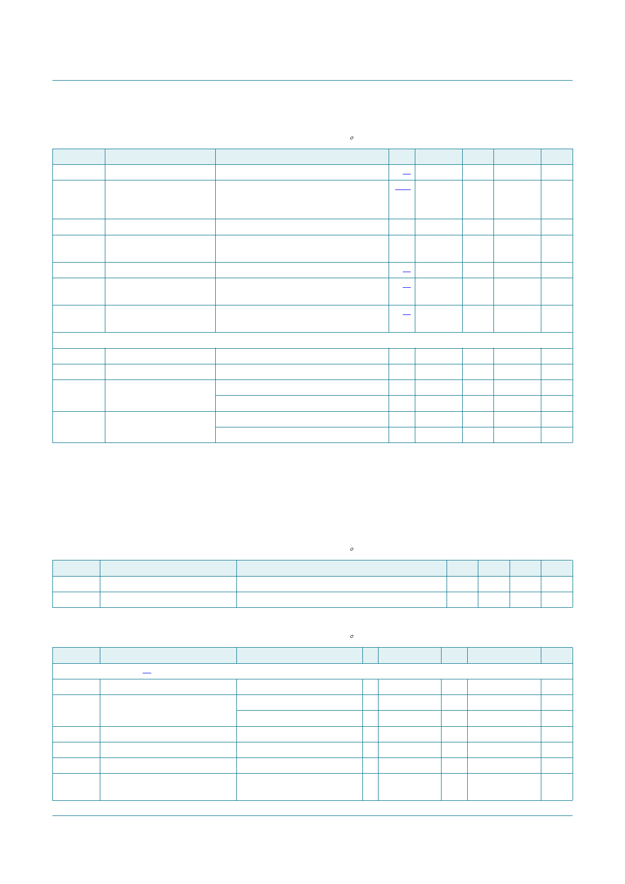
Table 18. Card drivers …continued
VDD = 3.3 V; VDD(INTF) = 1.5 V; fCLKIN = 10 MHz; GND = 0 V; Tamb = 25 C; unless otherwise specified.
Symbol Parameter
Conditions
Min
Typ
Max
Unit
Ipu
pull-up current
td
delay time
at pin I/O; VOH = 0.9VCC; CL = 30 pF
between edges on pin I/O and pin
I/OUC; corresponds to width of active
pull-up pulse
[3] 1
[3][4] -
-
-
mA
500 650
ns
tr
tR and tF
rise time
IO rise anf fall time
Ci
Rpu(int)
input capacitance
internal pull-up
resistance
inputs; from VIL(max) to VIH(min)
output transition time; from 10 % of VCC
to 90 % of VCC; CL < 30 pF; no DC load
on pin I/O
between pin I/O and VCC
-
-
[3] -
[3] 10
-
1.5
s
-
0.1
s
-
10
pF
13.5 17
k
fmax
maximum input clock on pin I/O
frequency
[3] -
-
500
kHz
Card presence input: pin PRES, active-HIGH when pin SPRES = LOW or active-LOW when pin SPRES = HIGH
VIL
LOW-level input voltage
VIH
HIGH-level input voltage
ILIL
LOW-level input leakage VI = 0.3VDD; pin SPRES = HIGH
current
VI = 0.3VDD; pin SPRES = LOW
ILIH
HIGH-level input
leakage current
VI = 0.7VDD; pin SPRES = HIGH
VI = 0.7VDD; pin SPRES = LOW
-
-
0.7VDD -
0
-
10
-
40
-
5
-
0.3VDD V
-
V
5
A
40
A
10
A
0
A
[1] Two ceramic multilayer capacitors of minimum 100 nF with low Equivalent Series Resistance (ESR) should be used in order to meet
these specifications.
[2] Output voltage towards the card, including ripple.
[3] Pin I/O has an internal 15 k pull-up resistor to VCC.
[4] Pin I/OUC has an internal 11 k pull-up resistor to VDD(INTF).
Table 19. Sequencer and clock counter
VDD = 3.3 V; VDD(INTF) = 1.5 V; fCLKIN = 10 MHz; GND = 0 V; Tamb = 25 C; unless otherwise specified.
Symbol Parameter
Conditions
Min Typ
tact
activation time
total sequence
-
-
tdeact
deactivation time
total sequence
60 80
Max Unit
135 s
100 s
Table 20. Interface signals to host controller
VDD = 3.3 V; VDD(INTF) = 1.5 V; fCLKIN = 10 MHz; GND = 0 V; Tamb = 25 C; unless otherwise specified.
Symbol Parameter
Conditions
Min
Typ Max
Data line: pin I/OUC[1]
VOL
LOW-level output voltage
IOL = 1 mA
0
- 0.3
VOH
HIGH-level output voltage
no DC load
IOH < 10 A
VIL
LOW-level input voltage
0.9VDD(INTF) -
0.75VDD(INTF) -
0.3
-
VDD(INTF) + 0.2
VDD(INTF) + 0.2
0.25VDD(INTF)
VIH
HIGH-level input voltage
0.7VDD(INTF) -
VDD(INTF) + 0.3
IIL
LOW-level input current
VIL = 0 V
-
- 600
ILIH
HIGH-level input leakage
VIH = VDD(INTF)
current
-
- 10
Unit
V
V
V
V
V
A
A
TDA8023
Product data sheet
All information provided in this document is subject to legal disclaimers.
Rev. 2.0 — 24 June 2016
© NXP Semiconductors N.V. 2016. All rights reserved.
20 of 33
Share Link: 