PSB2132 Просмотр технического описания (PDF) - Siemens AG
Номер в каталоге
Компоненты Описание
производитель
PSB2132 Datasheet PDF : 95 Pages
| |||
PSB 2132
PSB 2134
Functional Description
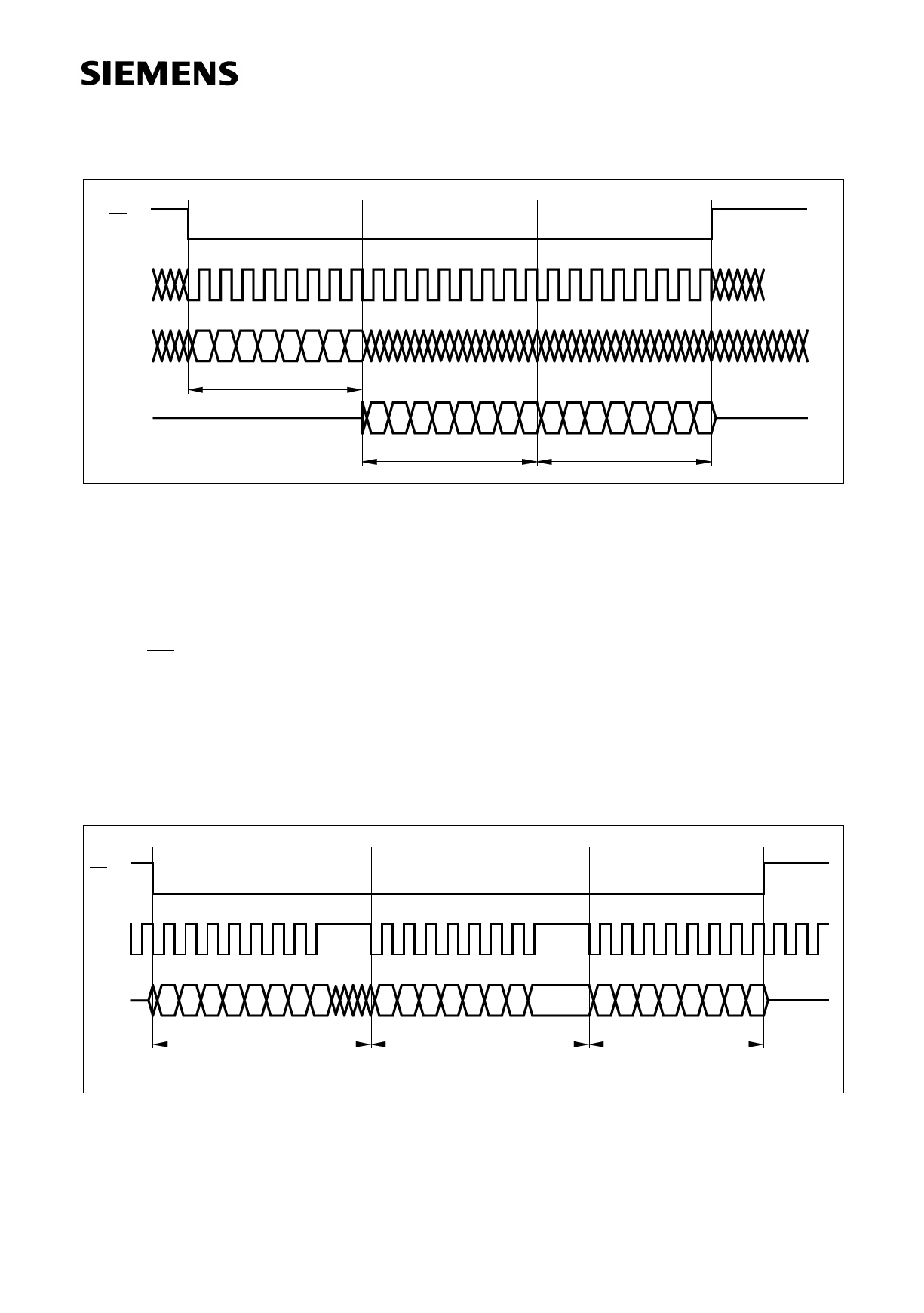
CS
DCLK
DIN
DOUT
76543210
Control
High ’Z’
7654321076543210
Identification
Data Byte 1
High ’Z’
ITD09771
Figure 7
Example for a Read Access, with One Data Byte Transferred via DOUT
The data transfer is synchronized by the DCLK input. The contents of DIN is latched at
the rising edge of DCLK, while DOUT changes with the falling edge of DCLK. During
execution of commands that are followed by output data (read commands), the device
will not accept any new command via DIN. The data transfer sequence is completed by
setting CS to high.
To reduce the number of connections to the µP DIN and DOUT may be strapped
together, and form a bi-directional data-‘pin’.
For special applications a byte by byte transfer is needed. This can be done by
prolonging the high time of DCLK for a user defined ‘waiting time’ after transferring any
byte.
CS
DCLK
DATA
76543210
Control-Byte
High ’Z’
7654321 0 76543210
Identification
Data Byte 1
ITD09772
Figure 8
Example for a Write/Read Access, with a Byte by Byte Transfer, and DIN and DOUT
Strapped Together
The Identification Byte is “81H” for the PSB 2132/34.
Semiconductor Group
20
09.97
Share Link: 