NCP367DPMEBTBG(2013) Просмотр технического описания (PDF) - ON Semiconductor
Номер в каталоге
Компоненты Описание
производитель
NCP367DPMEBTBG
(Rev.:2013)
(Rev.:2013)
ON Semiconductor
NCP367DPMEBTBG Datasheet PDF : 13 Pages
| |||
NCP367
240
220
200
180
160
140
120
100
80
0
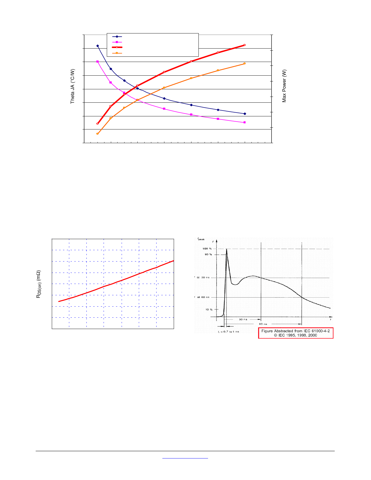
Theta JA curve with PCB cu thk 1.0 oz
Theta JA curve with PCB cu thk 2.0 oz
Power curve with PCB cu thk 2.0 oz
Power curve with PCB cu thk 1.0 oz
T_ambient
25°C
100
200
300
400
500
600
COPPER HEAT SPREADER AREA
(mm2)
Figure 14.
1.2
1.1
1
0.9
0.8
0.7
0.6
0.5
700
Internal PMOS FET
NCP367 includes an internal PMOS FET to protect the
systems, connected on OUT pin, from positive
over−voltage. Regarding electrical characteristics, the
RDS(on), during normal operation, will create low losses on
Vout pin versus Vin, due to very low RDS(on).
100
90
80
70
60
50
40
30
20
−50 −25
0
25 50 75
TEMPERATURE (°C)
100 125
Figure 15. Typical RDS(on) versus Temperature
ESD Tests
NCP367 fully support the IEC61000−4−2, level 4 (Input
pin, 1 mF mounted on board). That means, in Air condition,
Vin has a ±15 kV ESD protected input. In Contact condition,
Vin has ±8 kV ESD protected input. Please refer to Figure 16
to see the IEC 61000−4−2 electrostatic discharge waveform.
Figure 16. IEC 61000−4−2 Electrostatic Discharge
http://onsemi.com
11
Share Link: 