M5M29GB160BWG Просмотр технического описания (PDF) - MITSUBISHI ELECTRIC
Номер в каталоге
Компоненты Описание
производитель
M5M29GB160BWG
MITSUBISHI ELECTRIC
M5M29GB160BWG Datasheet PDF : 23 Pages
| |||
MITSUBISHI LSIs
M5M29GB/T161BWG
16,777,216-BIT (1048,576-WORD BY16-BIT)
CMOS 3.3V-ONLY, BLOCK ERASE FLASH MEMORY
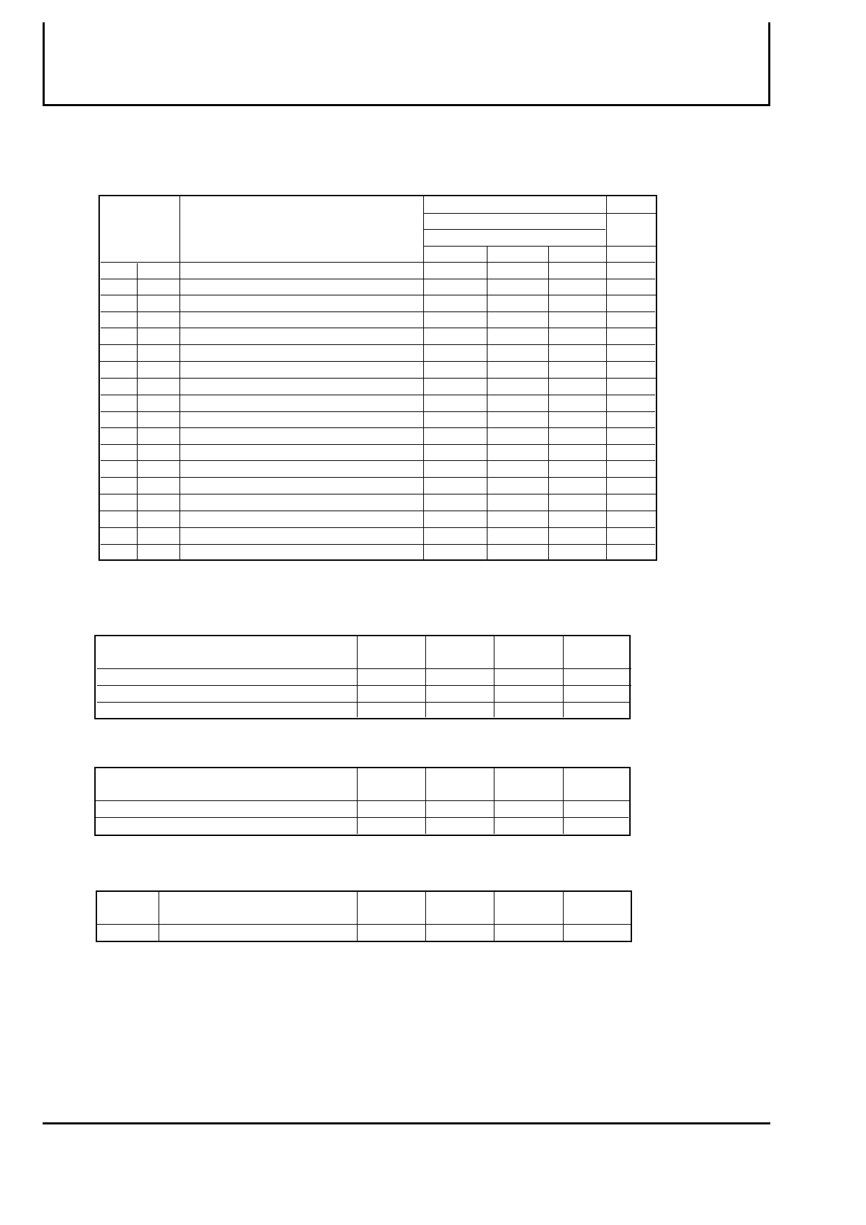
AC ELECTRICAL CHARACTERISTICS (Ta = -40 ~ 85°C, Vcc = 2.7V ~ 3.6V)
Write Mode (F-CE# control)
Limits
Symbol
Parameter
Vcc=2.7-3.6V
90ns
Unit
Min
Typ
Max
tWC tAVAV Write cycle time
90
ns
tAS tAVWH Address set-up time
50
ns
tAH tEHAX Address hold time
tDS tDVWH Data set-up time
0
ns
50
ns
tDH tEHDX Data hold time
0
ns
tOEH tEHGL OE# hold from CE# high
10
ns
tRE -
Latency between Read and Write FFH or 71H
30
ns
tWS tWLEL Write enable set-up time
0
ns
tWH tEHWH Write enable hold time
0
ns
tCEP tELEH CE# pulse width
60
ns
tCEPH tEHEL CE# pulse width high
30
ns
tGHEL tGHEL OE# hold to CE# Low
90
ns
tBLS tPHHEH Block Lock set-up to chip enable high
90
ns
tBLH tQVPH Block Lockhold from valid SRD
0
ns
tDAP tEHRH1 Duration of auto-program operation
4
80
ms
tDAE tEHRH2 Duration of auto-block erase operation
tEHRL tEHRL CE# high to F-RY/BY# low
40
600
ms
90
ns
tPS tPHWL RP# high recovery to write enable low
150
ns
Read timing parameters during command write operation mode are the same as during read-only operation mode.
Typical values at Vcc=3.3V, Ta=25°C
Erase and Program Performance
Parameter
Block Erase Time
Main Block Write Time (Page Mode)
Page Write Time
Min
Typ
Max
Unit
40
600
ms
1.0
1.8
sec
4
80
ms
Program Suspend Latency / Erase Suspend Time
Parameter
Program Suspend Latency
Erase Suspend Time
Please see page 19.
Min
Typ
Max
Unit
15
µs
15
µs
Vcc Power Up / Down Timing
Symbol
Parameter
Min
Typ
Max
Unit
tVCS
RP# =VIH set-up time from Vccmin
2
µs
Please see page 12.
During power up/down, by the noise pulses on control pins, the device has possibility of accidental erasure or programming.
The device must be protected against initiation of write cycle for memory contents during power up/down.
The delay time of min.2µsec is always required before read operation or write operation is initiated from the time Vcc reaches Vccmin during power up/down.
By holding RP# VIL, the contents of memory is protected during Vcc power up/down.
During power up, RP# must be held VIL for min.2µs from the time Vcc reaches Vccmin.
During power down, RP# must be held VIL until Vcc reaches GND.
RP# doesn't have latch mode ,therefore RP# must be held VIH during read operation or erase/program operation.
12
Sep.1999. Rev4.0
Share Link: 