M54123L-S08-R Просмотр технического описания (PDF) - Unisonic Technologies
Номер в каталоге
Компоненты Описание
производитель
M54123L-S08-R Datasheet PDF : 9 Pages
| |||
M54123L
LINEAR INTEGRATED CIRCUIT
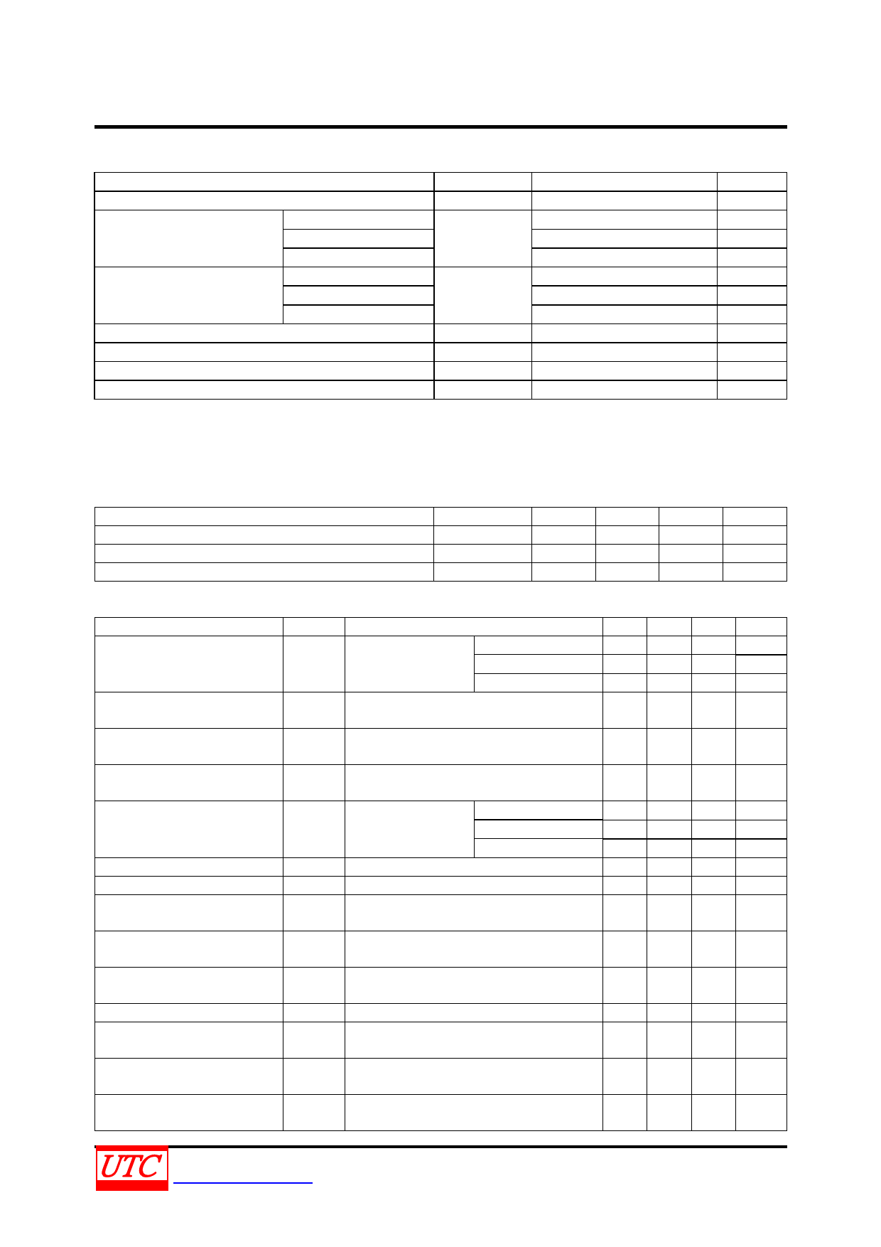
ABSOLUTE MAXIMUM RATING (unless otherwise specified)
PARAMETER
SYMBOL
RATINGS
UNIT
Supply Current
IS
8
mA
Between VR-IN (Note 2)
250
mA
VR Pin Current
Between VR-GND
IVR
30
mA
Between IN-VR(Note 2)
-250
mA
Between IN-VR(Note 2)
250
mA
IN Terminal Current
Between IN-GND
IIN
30
mA
Between VR-IN (Note 2)
-250
mA
SC Terminal Current
ISC
5
mA
Power Dissipation
PD
200
mW
Operating Temperature
TOPR
-20~ +80
°C
Storage Temperature
TSTG
-55~ +125
°C
Notes: 1. Absolute maximum ratings are those values beyond which the device could be permanently damaged.
Absolute maximum ratings are stress ratings only and functional device operation is not implied.
2. Current value between VR and IN, and between IN and VR is less than 1ms in the pulse width, and duty
cycle is less than 12%, In applying AC current continuously, it is 100 mA in the off-state.
RECOMMENDED OPERATING CONDITIONS (unless otherwise specified)
PARAMETER
SYMBOL
MIN
TYP
Supply Voltage When Latch Circuit Is Off-State
External Capacitor Between Vs and GND
External Capacitor Between Os and GND
VS
12
CVS
1
COS
ELECTRICAL CHARACTERISTICS (Ta=-20~+80°C, unless otherwise specified)
MAX
1
UNIT
V
μF
μF
PARAMETER
Supply Current
Trip Voltage
Timed Current1
Timed Current2
Output Current
SC “ON” Voltage (Note3)
SC Input Current
Output Low-Level Current
Input Clamp Voltage
Differential Input Clamp
Voltage
Maximum Current Voltage
Supply Current 2(Note 4)
Latch Circuit is Off-State
Supply Voltage (Note6)
Operating Time (Note 7)
SYMBOL
TEST CONDITIONS
Ta=-20°C
IS1
VS=12V,VR-VI=30mV
(See Test Circuit 1)
Ta=25°C
Ta=80°C
VT
VS=16V, VR-VI, Ta=-20~+80°C
(Note2) (See Test Circuit 2)
ITD1
Vs=16V, VR-VI=30mV, VOD=1.2V, Ta=25°C
(See Test Circuit 3)
ITD2
VS=16V, short circuit between VR and VI,
VOD=0.8V, Ta=25°C (See Test Circuit 4)
IO
VSC=1.4V,VOS=0.8V
(See Test Circuit 5)
IS1=580μA,Ta=-20°C
IS1=530μA,Ta=25°C
IS1=480μA,Ta=80°C
VSC(ON) VS=16V, Ta=25°C (See Test Circuit 6)
ISC(ON) VS=12V, Ta=25°C (See Test Circuit 7)
IOSL
VS=12V,VOSL=0.2V, Ta=-20~+80°C
(See Test Circuit 8)
VIC
VS=12V, IIC=20mA, Ta=-20~+80°C
(See Test Circuit 9)
VIDC
IIDC=100mA, Ta=-20~+80°C
(See Test Circuit 10)
VSM ISM=7mA, Ta=25°C (See Test Circuit 11)
IS2
VR-VI, VOS=0.6V, Ta=-20~+80°C
(Note 5) (See Test Circuit 12)
MIN
4
-12
17
-200
-100
-75
0.7
200
4.3
0.4
20
TYP
400
6.1
MAX
580
530
480
UNIT
μA
μA
μA
9 mVrms
-30 μA
37 μA
μA
μA
μA
1.4 V
5
μA
μA
6.7 V
2
V
28
V
1100 μA
VS(OFF) Ta=25°C (See Test Circuit 13)
0.5
V
TON
VS=16V,VR-VI=0.3V, Ta=25°C
(See Test Circuit 14)
2
4
ms
UNISONIC TECHNOLOGIES CO., LTD
www.unisonic.com.tw
4 of 9
QW-R122-001,D
Share Link: 