LT3013HFE Просмотр технического описания (PDF) - Linear Technology
Номер в каталоге
Компоненты Описание
производитель
LT3013HFE Datasheet PDF : 20 Pages
| |||
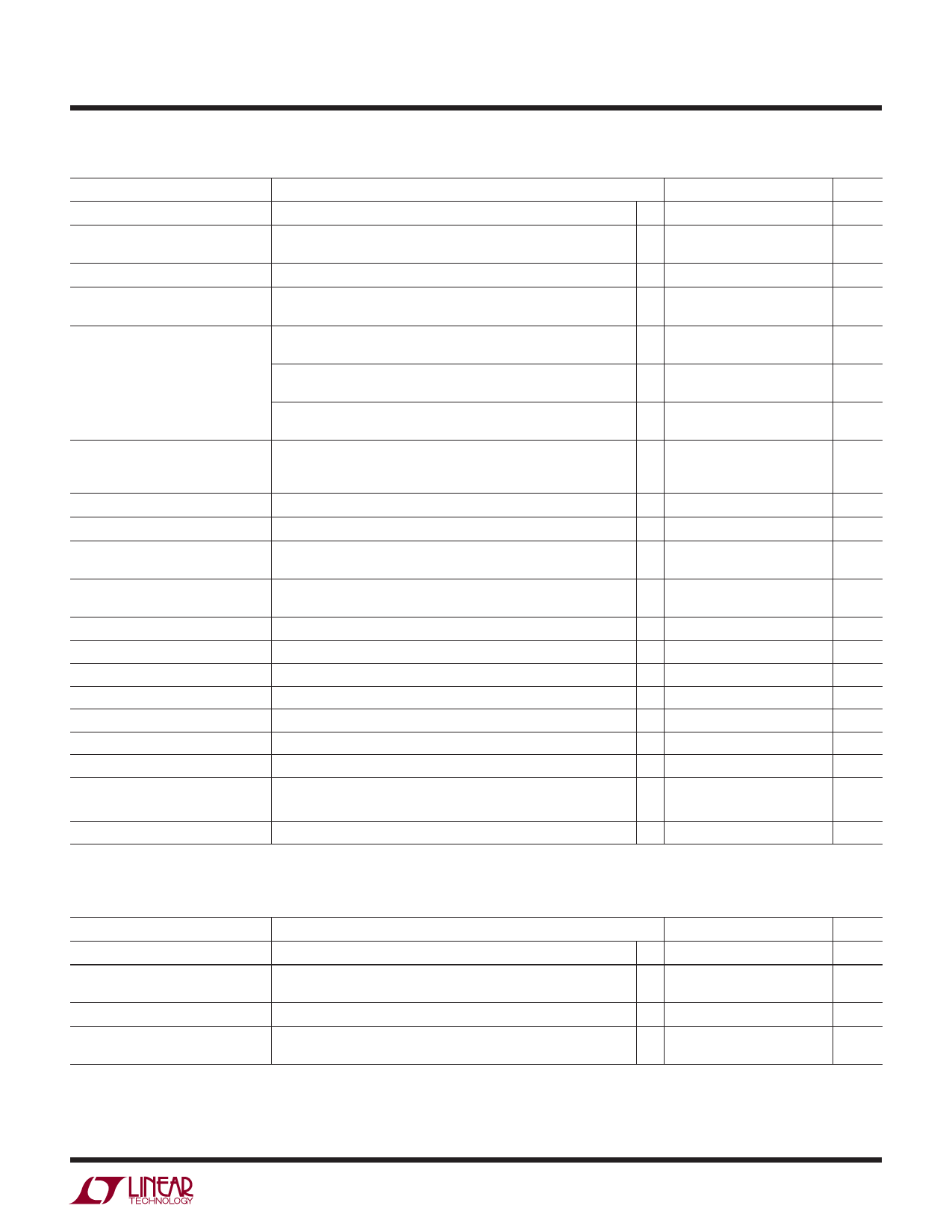
LT3013
ELECTRICAL CHARACTERISTICS (LT3013E, LT3013MP)
The l denotes the specifications which apply over the full operating temperature range, otherwise specifications are at TJ = 25°C.
PARAMETER
CONDITIONS
MIN TYP MAX
Minimum Input Voltage
ADJ Pin Voltage (Notes 2,3)
Line Regulation
Load Regulation (Note 2)
Dropout Voltage
VIN = VOUT(NOMINAL) (Notes 4, 5)
GND Pin Current
VIN = 4.75V
(Notes 4, 6)
Output Voltage Noise
ADJ Pin Bias Current
ILOAD = 250mA
VIN = 4V, ILOAD = 1mA
4.75V < VIN < 80V, 1mA < ILOAD < 250mA
ΔVIN = 4V to 80V, ILOAD = 1mA (Note 2)
VIN = 4.75V, ΔILOAD = 1mA to 250mA
VIN = 4.75V, ΔILOAD = 1mA to 250mA
ILOAD = 10mA
ILOAD = 10mA
ILOAD = 50mA
ILOAD = 50mA
ILOAD = 250mA
ILOAD = 250mA
ILOAD = 0mA
ILOAD = 100mA
ILOAD = 250mA
COUT = 10μF, ILOAD = 250mA, BW = 10Hz to 100kHz
(Note 7 )
l
4
4.75
1.225 1.24 1.255
l 1.2
1.24 1.28
l
0.1
5
7
12
l
25
160
230
l
300
250
340
l
420
400
490
l
620
l
65
120
3
l
10
18
100
30
100
Shutdown Threshold
SHDN Pin Current (Note 8)
Quiescent Current in Shutdown
PWRGD Trip Point
VOUT = Off to On
VOUT = On to Off
VSHDN = 0V
VSHDN = 6V
VIN = 6V, VSHDN = 0V
% of Nominal Output Voltage, Output Rising
l
1.3
2
l 0.3
0.8
0.3
2
0.1
1
1
5
l 85
90
94
PWRGD Trip Point Hysteresis
% of Nominal Output Voltage
1.1
PWRGD Output Low Voltage
CT Pin Charging Current
CT Pin Voltage Differential
Ripple Rejection
Current Limit
IPWRGD = 50μA
l
140
250
3.0
6
VCT(PWRGD High) – VCT(PWRGD Low)
1.6
VIN = 7V(Avg), VRIPPLE = 0.5VP-P, fRIPPLE = 120Hz, ILOAD = 250mA
65
75
VIN = 7V, VOUT = 0V
VIN = 4.75V, ΔVOUT = –0.1V (Note 2)
400
l 250
Reverse Output Current (Note 9)
VOUT = 1.24V, VIN < 1.24V (Note 2)
12
25
UNITS
V
V
V
mV
mV
mV
mV
mV
mV
mV
mV
mV
μA
mA
mA
μVRMS
nA
V
V
μA
μA
μA
%
%
mV
μA
V
dB
mA
mA
μA
ELECTRICAL CHARACTERISTICS (LT3013H)
The l denotes the specifications which apply over the –40°C to 140°C operating temperature range, otherwise specifications are at TJ = 25°C.
PARAMETER
CONDITIONS
MIN TYP MAX UNITS
Minimum Input Voltage
ILOAD = 200mA
l
4
4.75
V
ADJ Pin Voltage (Notes 2,3)
Line Regulation
VIN = 4V, ILOAD = 1mA
4.75V < VIN < 80V, 1mA < ILOAD < 200mA
ΔVIN = 4V to 80V, ILOAD = 1mA (Note 2)
1.225 1.24 1.255
V
l 1.2
1.24 1.28
V
l
0.1
5
mV
Load Regulation (Note 2)
VIN = 4.75V, ΔILOAD = 1mA to 200mA
VIN = 4.75V, ΔILOAD = 1mA to 200mA
6
12
mV
l
30
mV
3013fe
3
Share Link: 