IDT72V3641 Просмотр технического описания (PDF) - Integrated Device Technology
Номер в каталоге
Компоненты Описание
производитель
IDT72V3641 Datasheet PDF : 21 Pages
| |||
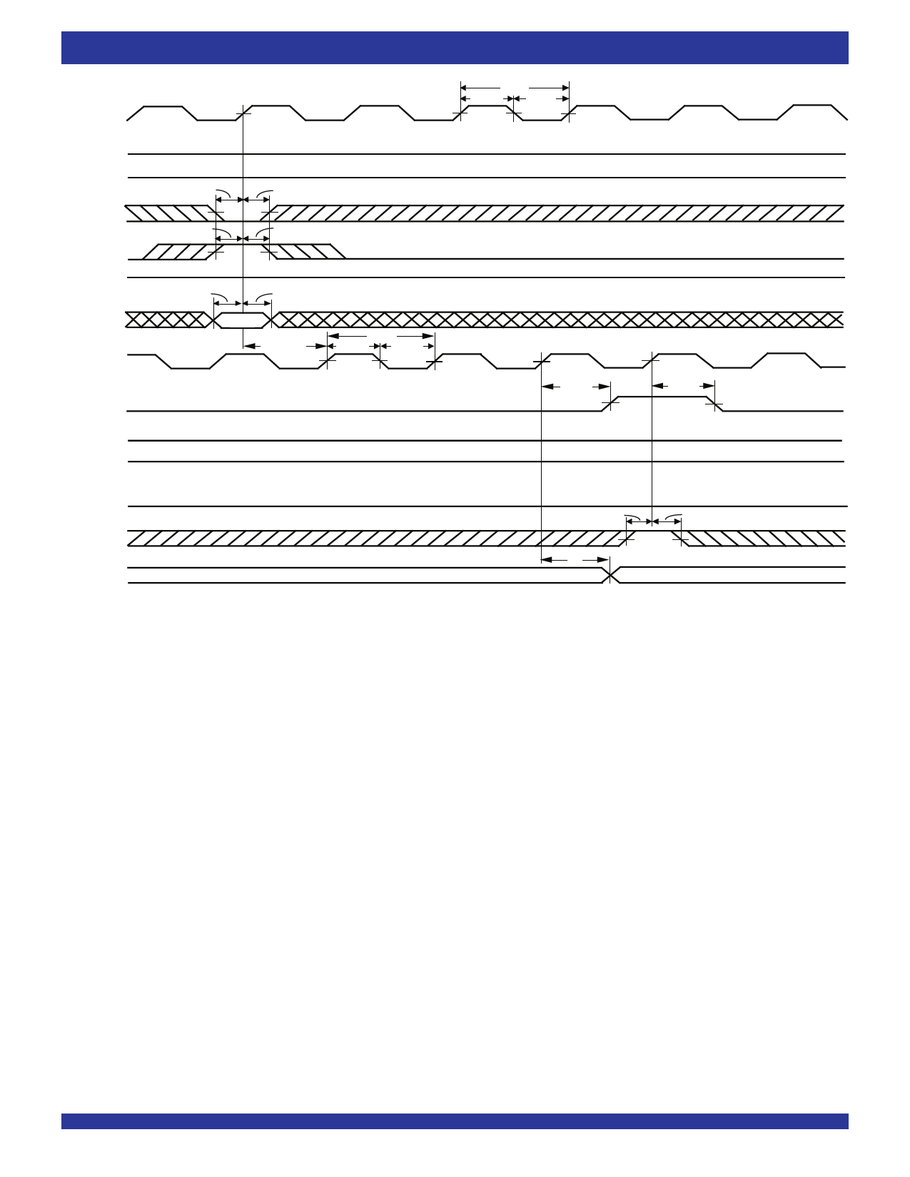
IDT72V3631/72V3641/72V3651
3.3V CMOS SYNCFIFO™ 512 x 36, 1,024 x 36 and 2,048 x 36
CLKA
CSA LOW
tCLK
tCLKH tCLKL
COMMERCIAL TEMPERATURE RANGE
W/RA HIGH
MBA
ENA
tENS2
tENS1
tENH2
tENH1
IR HIGH
tDS
tDH
A0 - A35
CLKB
W1
tSKEW1 (1)
tCLK
tCLKH tCLKL
1
2
OR FIFO Empty
CSB LOW
3
tPOR
tPOR
W/RB HIGH
MBB LOW
ENB
B0 -B35
Old Data in FIFO Output Register
tENS1
tA
tENH1
W1
4658 drw 10
NOTE:
1. tSKEW1 is the minimum time between a rising CLKA edge and a rising CLKB edge for OR to transition HIGH and to clock the next word to the FIFO output register in three CLKB cycles.
If the time between the rising CLKA edge and rising CLKB edge is less than tSKEW1, then the transition of OR HIGH and the first word load to the output register may occur one CLKB cycle
later than shown.
Figure 7. OR Flag Timing and First Data Word Fall Through when the FIFO is Empty
15
Share Link: 