IDT7202LA30TDI(1997) Просмотр технического описания (PDF) - Integrated Device Technology
Номер в каталоге
Компоненты Описание
производитель
IDT7202LA30TDI
(Rev.:1997)
(Rev.:1997)
Integrated Device Technology
IDT7202LA30TDI Datasheet PDF : 13 Pages
| |||
IDT7200/7201A/7202A CMOS ASYNCHRONOUS FIFO
256 x 9, 512 x 9 and 1,024 x 9
MILITARY, INDUSTRIAL AND COMMERCIAL TEMPERATURE RANGES
DC ELECTRICAL CHARACTERISTICS
(Commercial: VCC = 5V ± 10%, TA = 0°C to +70°C; Industrial: VCC = 5V ± 10%, TA = –40°C to +85°C; Military: VCC = 5V ± 10%, TA = –55°C to +125°C)
IDT7200L
IDT7201LA
IDT7202LA
Com'l & Ind'l(1)
tA = 12, 15, 20, 25, 35 ns
IDT7200L
IDT7201LA
IDT7202LA
Military
tA = 20, 30, 40 ns
Symbol
ILI(2)
ILO(3)
Parameter
Input Leakage Current (Any Input)
Output Leakage Current
Min.
–1
–10
Typ.
—
—
Max.
1
10
Min.
–10
–10
Typ.
—
—
Max. Unit
10 µA
10 µA
VOH
Output Logic “1” Voltage IOH = –2mA
2.4
—
—
2.4
—
—
V
VOL
ICC1(4,5,6)
ICC2(4,6,7)
ICC3(L)(4,6,7)
Output Logic “0” Voltage IOL = 8mA
Active Power Supply Current
Standby Current (R=W=RS=FL/RT=VIH)
Power Down Current
—
—
0.4
—
—
—
125
—
—
—
15
—
—
—
0.5
—
—
0.4
V
—
140 mA
—
20 mA
—
0.9 mA
2679 tbl 04
Symbol
ILI(2)
ILO(3)
VOH
VOL
ICC1(4,5,6)
ICC2(4,6,7)
ICC3(L)(4,6,7)
Parameter
Input Leakage Current (Any Input)
Output Leakage Current
Output Logic “1” Voltage IOH = –2mA
Output Logic “0” Voltage IOL = 8mA
Active Power Supply Current
Standby Current (R=W=RS=FL/RT=VIH)
Power Down Current
Min.
–1
–10
2.4
—
—
—
—
IDT7200L
IDT7201LA
IDT7202LA
Commercial
tA = 50 ns
Typ.
Max.
—
1
—
10
—
—
—
0.4
50
80
5
8
—
0.5
IDT7200L
IDT7201LA
IDT7202LA
Military
tA = 50, 65, 80, 120 ns
Min.
Typ.
Max. Unit
–10
—
10 µA
–10
—
10 µA
2.4
—
—
V
—
—
0.4
V
—
70
100 mA
—
8
15 mA
—
—
0.9 mA
NOTES:
2679 tbl 05
1. Industrial temperature range product for the 25 ns speed grade is available as a standard device. All other speed grades are available by special order.
2. Measurements with 0.4 ≤ VIN ≤ VCC.
3. R ≥ VIH, 0.4 ≤ VOUT ≤ VCC.
4. Tested with outputs open (IOUT = 0).
5. RCLK and WCLK toggle at 20 MHz and data inputs switch at 10 MHz.
6. ICC measurements are made with outputs open.
7. All Inputs = VCC - 0.2V or GND + 0.2V, except RCLK and WCLK, which toggle at 20 MHz.
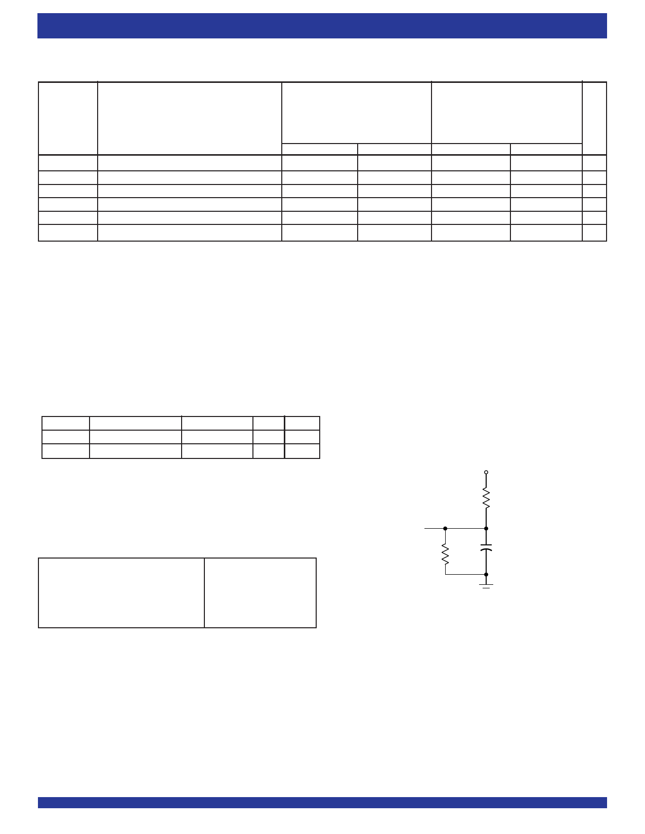
AC TEST CONDITIONS
Input Pulse Levels
Input Rise/Fall Times
Input Timing Reference Levels
Output Reference Levels
Output Load
GND to 3.0V
5ns
1.5V
1.5V
See Figure 1
2679 tbl 08
3
Share Link: 