MCM6205DJ15 Просмотр технического описания (PDF) - Motorola => Freescale
Номер в каталоге
Компоненты Описание
производитель
MCM6205DJ15 Datasheet PDF : 8 Pages
| |||
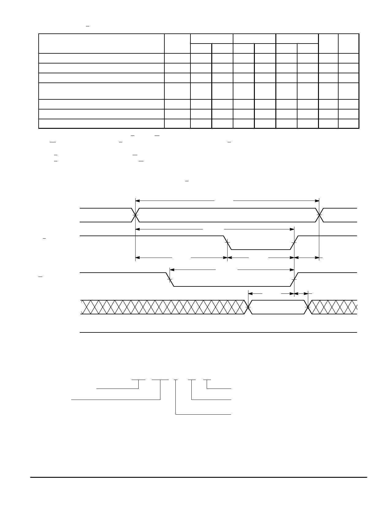
WRITE CYCLE 2 (E Controlled, See Notes 1 and 2)
MCM6205D–15 MCM6205D–20 MCM6205D–25
Parameter
Symbol Min Max Min Max Min Max Unit Notes
Write Cycle Time
tAVAV
15
—
20
—
25
—
ns
3
Address Setup Time
Address Valid to End of Write
tAVEL
0
—
0
—
0
—
ns
tAVEH
12
—
15
—
20
—
ns
Enable to End of Write
tELEH, 10
—
12
—
15
—
ns 4, 5
tELWH
Data Valid to End of Write
tDVEH
7
—
8
—
10
—
ns
Data Hold Time
tEHDX
0
—
0
—
0
Write Recovery Time
tEHAX
0
—
0
—
0
NOTES:
1. A write occurs during the overlap of E low and W low.
2. E1 and E2 are represented by E in this data sheet. E2 is of opposite polarity to E.
3. All timings are referenced from the last valid address to the first transitioning address.
4. If E goes low coincident with or after W goes low, the output will remain in a high impedance state.
5. If E goes high coincident with or before W goes high, the output will remain in a high impedance state.
—
ns
—
ns
A (ADDRESS)
E (CHIP ENABLE)
W (WRITE ENABLE)
D (DATA IN)
WRITE CYCLE 2 (E Controlled, See Notes 1 and 2)
tAVAV
tAVEL
tAVEH
tWLEH
tELEH
tELWH
tDVEH
DATA VALID
tEHAX
tEHDX
Q (DATA OUT)
HIGH–Z
Motorola Memory Prefix
Part Number
ORDERING INFORMATION
(Order by Full Part Number)
MCM 6205D X XX XX
Shipping Method (R2 = Tape and Reel, Blank = Rails)
Speed (15 = 15 ns, 20 = 20 ns, 25 = 25 ns)
Package (J = 300 mil SOJ)
Full Part Numbers — MCM6205DJ15
MCM6205DJ20
MCM6205DJ25
MCM6205DJ15R2
MCM6205DJ20R2
MCM6205DJ25R2
MCM6205D
6
MOTOROLA FAST SRAM
Share Link: 