74LVC32244A Просмотр технического описания (PDF) - Philips Electronics
Номер в каталоге
Компоненты Описание
производитель
74LVC32244A Datasheet PDF : 16 Pages
| |||
Philips Semiconductors
32-bit buffer/line driver; 5 V input/output
tolerant; 3-state
Product specification
74LVC32244A;
74LVCH32244A
FEATURES
• 5 V tolerant inputs/outputs for interfacing with 5 V logic
• Wide supply voltage range of 1.2 to 3.6 V
• CMOS low power consumption
• MULTIBYTE™ flow-trough standard pin-out architecture
• Low inductance multiple power and ground pins for
minimum noise and ground bounce
• Direct interface with TTL levels
• Bus hold on data inputs (74LVCH32244A only)
• Typical output ground bounce voltage:
VOLP <0.8 V at VCC = 3.3 V; Tamb = 25 °C
• Typical output VOH undershoot voltage:
VOHV >2 V at VCC = 3.3 V; Tamb = 25 °C
• Power-off disabled outputs, permitting live insertion
• Plastic fine-pitch ball grid array package.
DESCRIPTION
The 74LVC(H)32244A is a high-performance, low-power,
low-voltage, Si-gate CMOS device, superior to most
advanced CMOS compatible TTL families. Inputs can be
driven from either 3.3 or 5 V devices. In 3-state operation,
outputs can handle 5 V. These features allow the use of
these devices in a mixed 3.3 and 5 V environment.
The 74LVC(H)32244A is a 32-bit non-inverting buffer/line
driver with 3-state outputs. The 3-state outputs are
controlled by the output enable inputs 1OE and 2OE.
A HIGH on input nOE causes the outputs to assume a
high-impedance OFF-state.
To ensure the high-impedance state during power-up or
power-down, input nOE should be tied to VCC through a
pull-up resistor; the minimum value of the resistor is
determined by the current-sinking capability of the driver.
The 74LVCH32244A bus hold data input circuit eliminates
the need for external pull-up resistors to hold unused or
floating data inputs at a valid logic level (see Fig.3).
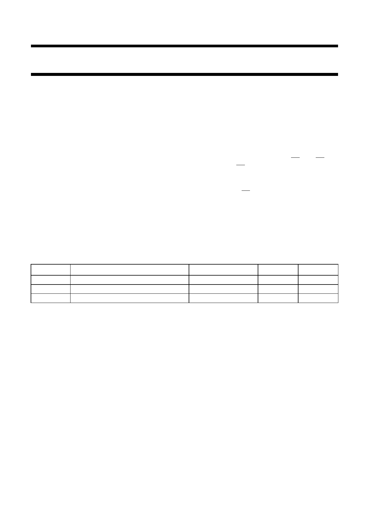
QUICK REFERENCE DATA
Ground = 0 V; Tamb = 25 °C; tr = tf ≤ 2.5 ns.
SYMBOL
tPHL/tPLH
CI
CPD
PARAMETER
propagation delay nAn to nYn
input capacitance
power dissipation capacitance per buffer
CONDITIONS
TYPICAL
CL = 50 pF; VCC = 3.3 V 3.0
5.0
VI = GND to VCC; note 1 25
Note
1. CPD is used to determine the dynamic power dissipation (PD in µW).
PD = CPD × VCC2 × fi + Σ(CL × VCC2 × fo) where:
fi = input frequency in MHz;
fo = output frequency in MHz;
CL = output load capacitance in pF;
VCC = supply voltage in Volts;
Σ(CL × VCC2 × fo) = sum of the outputs.
UNIT
ns
pF
pF
1999 Aug 31
2
Share Link: 