BLF573 Просмотр технического описания (PDF) - NXP Semiconductors.
Номер в каталоге
Компоненты Описание
производитель
BLF573 Datasheet PDF : 16 Pages
| |||
NXP Semiconductors
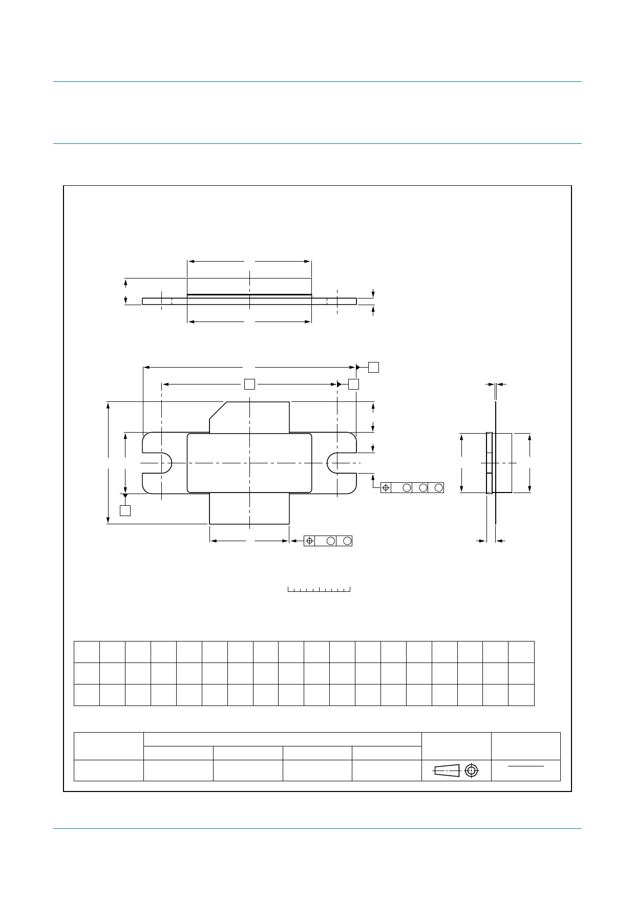
9. Package outline
Flanged LDMOST ceramic package; 2 mounting holes; 2 leads
BLF573; BLF573S
HF / VHF power LDMOS transistor
SOT502A
D
A
F
3
D1
U1
B
q
C
c
1
L
H U2
A
2
b
p
E1
E
w1 M A M B M
w2 M C M
Q
0
5 10 mm
scale
DIMENSIONS (millimetre dimensions are derived from the original inch dimensions)
UNIT A
b
c
D D1
E
E1
F
H
L
p
Q
q
U1 U2 w1 w2
mm
4.72 12.83 0.15 20.02 19.96 9.50
3.43 12.57 0.08 19.61 19.66 9.30
9.53
9.25
1.14 19.94 5.33
0.89 18.92 4.32
3.38
3.12
1.70
1.45
27.94 34.16
33.91
9.91
9.65
0.25
0.51
inches
0.186
0.135
0.505 0.006
0.495 0.003
0.788 0.786
0.772 0.774
0.374 0.375
0.366 0.364
0.045 0.785
0.035 0.745
0.210 0.133
0.170 0.123
0.067
0.057
1.100
1.345
1.335
0.390
0.380
0.01
0.02
OUTLINE
VERSION
IEC
SOT502A
REFERENCES
JEDEC
JEITA
Fig 11. Package outline SOT502A
BLF573_BLF573S
Product data sheet
All information provided in this document is subject to legal disclaimers.
Rev. 3 — 8 July 2010
EUROPEAN
PROJECTION
ISSUE DATE
99-12-28
03-01-10
© NXP B.V. 2010. All rights reserved.
11 of 16
Share Link: 