ATF-53189 Просмотр технического описания (PDF) - Avago Technologies
Номер в каталоге
Компоненты Описание
производитель
ATF-53189 Datasheet PDF : 17 Pages
| |||
Input Matching Circuit
Input
Γ_mag=0.74
DUT
Γ_ang=-112.4°
Output Matching Circuit
Γ_mag=0.40
Γ_ang=120.0°
Output
Figure 1. Block diagram of the 2 GHz production test board used for NF, Gain, OIP3 , P1dB, PAE and
ACLR measurements. This circuit achieves a trade-off between optimal OIP3, P1dB and VSWR. Circuit
losses have been de-embedded from actual measurements.
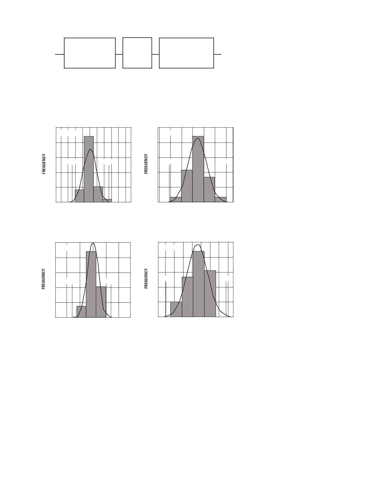
Product Consistency Distribution Charts [1,2]
150
Stdev=0.86
120
150
Stdev=0.08
120
90
–3 Std
60
+3 Std
90
–3 Std
60
+3 Std
30
30
0
36 37 38 39 40 41 42 43 44 45
OIP3 (dBm)
Figure 2. OIP3 @ 2 GHz, 4V, 135 mA.
LSL = 36 dBm, Nominal = 40 dBm.
0
.5 .6 .7 .8 .9 1 1.1
NF (dB)
Figure 3. NF @ 2 GHz, 4V, 135 mA.
USL = 1.30 dBm, Nominal = 0.84 dBm.
150
Stdev=0.22
120
150
Stdev=1.14
120
90
–3 Std
60
+3 Std
90
–3 Std
60
+3 Std
30
30
0
14.5 15 15.5 16 16.5
Gain (dB)
Figure 4. Gain @ 2 GHz, 4V, 135 mA.
LSL = 14 dBm, Nominal = 15.5 dBm,
USL = 17 dBm.
0
19 20 21 22 23 24 25 26
P1dB (dBm)
Figure 5. P1dB @ 2 GHz, 4V, 135 mA.
Nominal = 23 dBm.
Notes:
1. Distribution data sample size is 500 samples taken from 3 different wafers. Future wafers
allocated to this product may have nominal values anywhere between the upper and lower
limits.
2. Measurements are made on production test board, which represents a trade-off between
optimal OIP3, P1dB and VSWR. Circuit losses have been de‑embedded from actual measure-
ments.
3
Share Link: 