ADT7517ARQ Просмотр технического описания (PDF) - Analog Devices
Номер в каталоге
Компоненты Описание
производитель
ADT7517ARQ
Analog Devices
ADT7517ARQ Datasheet PDF : 44 Pages
| |||
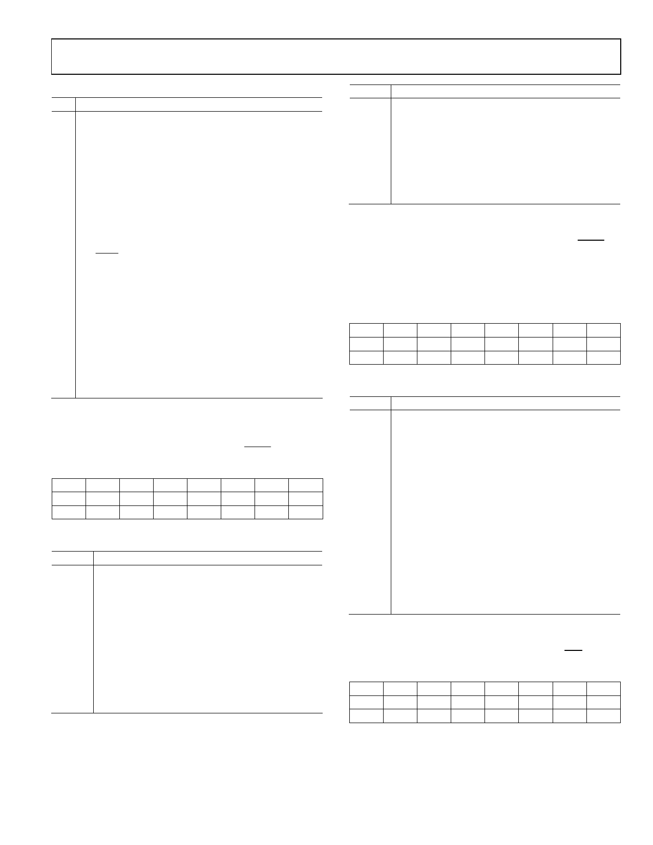
Table 18.
Bit Function
C0 Selects between fast and slow ADC conversion speeds.
0 = ADC clock at 1.4 kHz.
1 = ADC clock at 22.5 kHz. D+ and D– analog filters are
disabled.
C1 On the ADT7516 and ADT7517, this bit selects between
8-bit and 10-bit DAC output resolution on the thermal
voltage output feature. The default is 8 bits. This bit has no
effect on the ADT7519 output because this part has only
an 8-bit DAC. For the ADT7519, write 0 to this bit.
0 = 8-bit resolution.
1 = 10-bit resolution.
C2 Reserved. Write 0 only.
C3 0 = LDAC pin controls updating of DAC outputs.
1 = DAC configuration register and LDAC configuration
register control updating of DAC outputs.
C4 Selects the ADC reference to be either internal VREF or VDD
for analog inputs.
0 = internal VREF.
1 = VDD.
C5 Setting this bit selects DAC A voltage output to be
proportional to the internal temperature measurement.
C6 Setting this bit selects DAC B voltage output to be
proportional to the external temperature measurement.
C7 Reserved. Write 0 only.
DAC Configuration Register (Read/Write) [Address = 0x1B]
This configuration register is an 8-bit read/write register that is
used to control the output ranges of all four DACs and also to
control the loading of the DAC registers if the LDAC pin is
disabled (Bit C3 = 1, Control Configuration 3 register).
D7 D6 D5 D4 D3 D2 D1 D0
D7 D6 D5 D4 D3 D2 D1 D0
01
01
01
01
01
01
01
01
1 Default settings at power-up.
Table 19.
Bit
Function
D0
Selects the output range of DAC A.
0 = 0 V to VREF.
1 = 0 V to 2 VREF.
D1
Selects the output range of DAC B.
0 = 0 V to VREF.
1 = 0 V to 2 VREF.
D2
Selects the output range of DAC C.
0 = 0 V to VREF.
1 = 0 V to 2 VREF.
D3
Selects the output range of DAC D.
0 = 0 V to VREF.
1 = 0 V to 2 VREF.
ADT7516/ADT7517/ADT7519
Bit
[D4:D5]
[D6:D7]
Function
00 = MSB write to any DAC register generates LDAC
command that updates that DAC only.
01 = MSB write to DAC B or DAC D register generates
LDAC command that updates DAC A and DAC B or
DAC C and DAC D, respectively.
10 = MSB write to DAC D register generates LDAC
command that updates all four DACs.
11 = LDAC command generated from LDAC register.
Reserved. Write 0s only.
LDAC Configuration Register (Write-Only)[Address = 0x1C]
This configuration register is an 8-bit write register that is used
to control the updating of the quad DAC outputs if the LDAC
pin is disabled and Bits[D4:D5] of the DAC configuration
register are both set to 1. Also selects either the internal or the
external VREF for all four DACs. Bits[D0:D3] in this register are
self-clearing, that is, reading back from this register always gives
0s for these bits.
D7 D6 D5 D4 D3 D2 D1 D0
D7 D6 D5 D4 D3 D2 D1 D0
01
01
01
01
01
01
01
01
1 Default settings at power-up.
Table 20.
Bit
Function
D0
Writing a 1 to this bit generates the LDAC command
to update DAC A output only.
D1
Writing a 1 to this bit generates the LDAC command
to update DAC B output only.
D2
Writing a 1 to this bit generates the LDAC command
to update DAC C output only.
D3
Writing a 1 to this bit generates the LDAC command
to update DAC D output only.
D4
Selects either internal VREF or external VREF for DAC A
and DAC B.
0 = external VREF.
1 = internal VREF.
D5
Selects either internal VREF or external VREF for DAC C
and DAC D.
0 = external VREF.
1 = internal VREF.
[D6:D7] Reserved. Write 0s only.
Interrupt Mask 1 Register (Read/Write) [Address = 0x1D]
This mask register is an 8-bit read/write register that can be
used to mask any interrupts that can cause the INT/INT pin to
go active.
D7 D6 D5 D4 D3 D2 D1 D0
D7 D6 D5 D4 D3 D2 D1 D0
01
01
01
01
01
01
01
01
1 Default settings at power-up.
Rev. B | Page 33 of 44
Share Link: 