ADSP-21469KBCZ-4(Rev0) Просмотр технического описания (PDF) - Analog Devices
Номер в каталоге
Компоненты Описание
производитель
ADSP-21469KBCZ-4 Datasheet PDF : 72 Pages
| |||
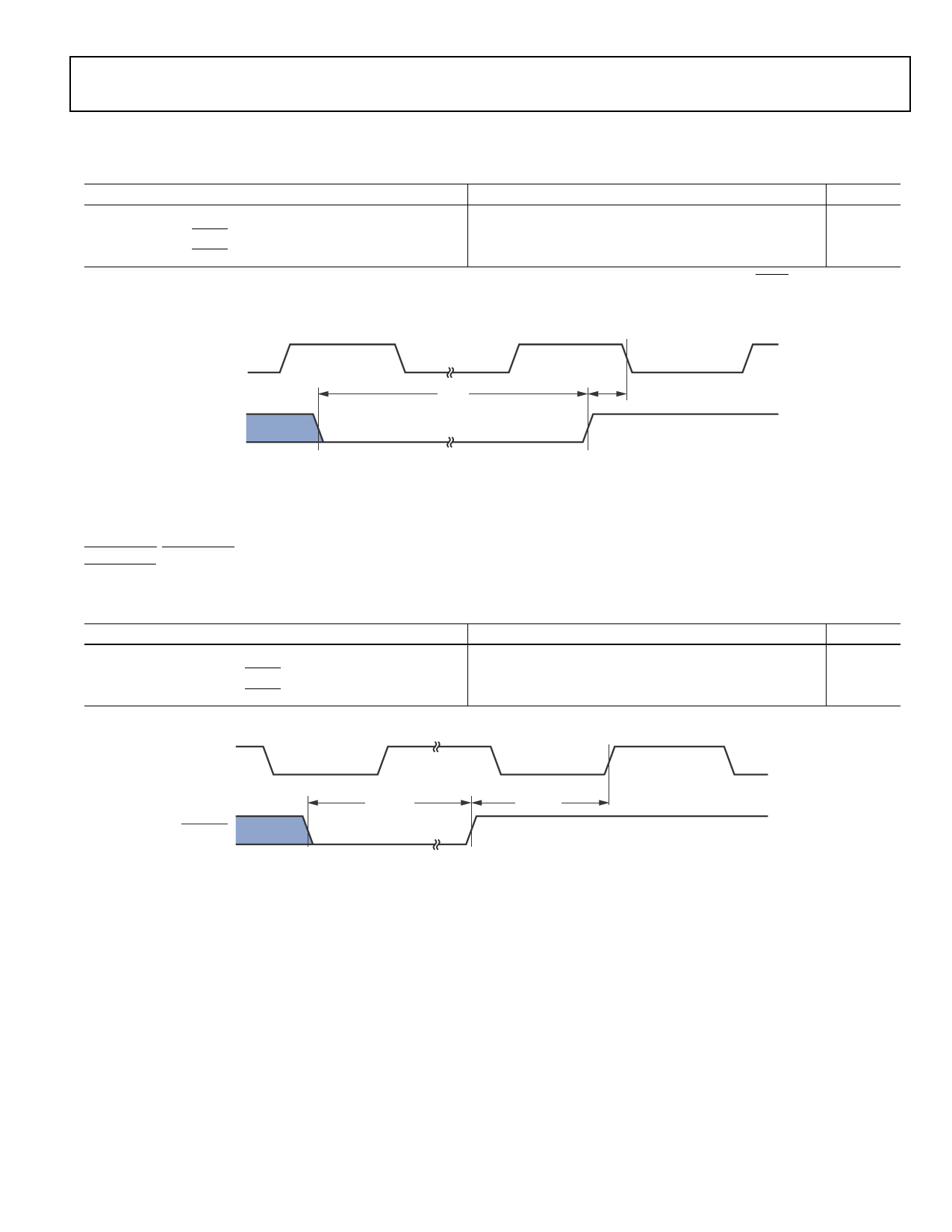
Timer PWM_OUT Cycle Timing
The following timing specification applies to Timer0 and
Timer1 in PWM_OUT (pulse-width modulation) mode. Timer
signals are routed to the DPI_P14–1 pins through the DPI SRU.
Therefore, the timing specifications provided below are valid at
the DPI_P14–1 pins.
Table 23. Timer PWM_OUT Timing
Parameter
Switching Characteristic
tPWMO
Timer Pulse Width Output
Min
2 × tPCLK – 1.2
PWM
OUTPUTS
tPWMO
Figure 13. Timer PWM_OUT Timing
Timer WDTH_CAP Timing
The following timing specification applies to Timer0 and
Timer1 in WDTH_CAP (pulse width count and capture) mode.
Timer signals are routed to the DPI_P14–1 pins through the
SRU. Therefore, the timing specifications provided below are
valid at the DPI_P14–1 pins.
Table 24. Timer Width Capture Timing
Parameter
Timing Requirement
tPWI
Timer Pulse Width
Min
2 × tPCLK
TIMER
CAPTURE
INPUTS
tPWI
Figure 14. Timer Width Capture Timing
ADSP-21469
Max
2 × (231 – 1) × tPCLK
Unit
ns
Max
2 × (231 – 1) × tPCLK
Unit
ns
Rev. 0 | Page 27 of 72 | June 2010
Share Link: 