74ABT374CMSA(2005) Просмотр технического описания (PDF) - Fairchild Semiconductor
Номер в каталоге
Компоненты Описание
производитель
74ABT374CMSA Datasheet PDF : 11 Pages
| |||
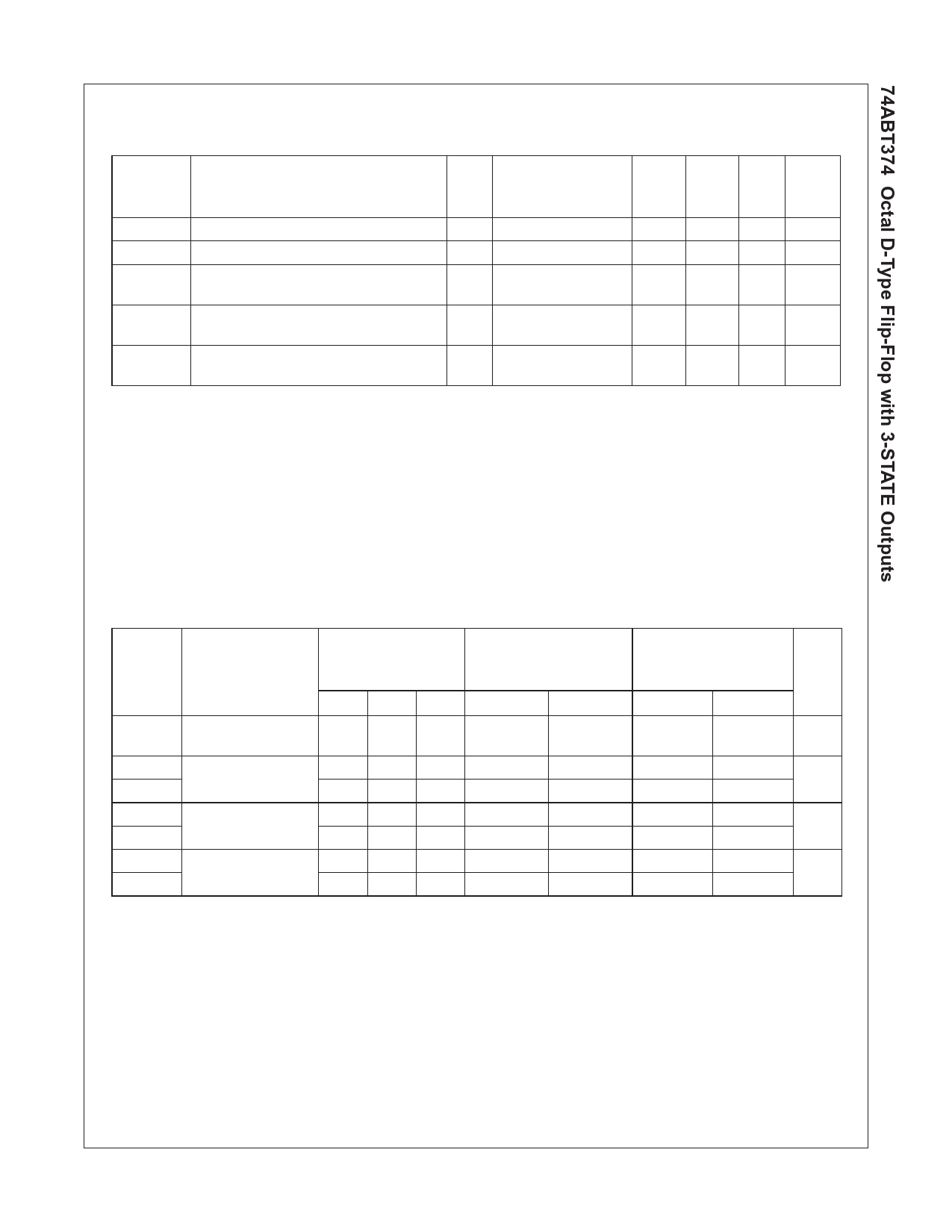
Extended AC Electrical Characteristics
(SOIC Package)
TA 40qC to 85qC
TA 40qC to 85qC
TA 40qC to 85qC
VCC 4.5V to 5.5V
VCC 4.5V to 5.5V
VCC 4.5V to 5.5V
Symbol
Parameter
CL 50 pF
8 Outputs Switching
CL 250 pF
(Note 10)
CL 250 pF
8 Outputs Switching
Units
(Note 9)
(Note 11)
Min
Max
Min
Max
Min
Max
tPLH
Propagation Delay
tPHL
CP to On
1.5
5.7
2.0
7.8
2.0
10.0
ns
1.5
5.7
2.0
7.8
2.0
10.0
tPZH
Output Enable Time
tPZL
1.5
6.2
2.0
8.0
2.0
10.5
ns
1.5
6.2
2.0
8.0
2.0
10.5
tPHZ
tPZL
Output Disable Time
1.0
5.5
1.0
5.5
(Note 12)
(Note 12)
ns
Note 9: This specification is guaranteed but not tested. The limits apply to propagation delays for all paths described switching in phase
(i.e., all LOW-to-HIGH, HIGH-to-LOW, etc.).
Note 10: This specification is guaranteed but not tested. The limits represent propagation delay with 250 pF load capacitors in place of the 50 pF load capac-
itors in the standard AC load. This specification pertains to single output switching only.
Note 11: This specification is guaranteed but not tested. The limits represent propagation delays for all paths described switching in phase
(i.e., all LOW-to-HIGH, HIGH-to-LOW, etc.) with 250 pF load capacitors in place of the 50 pF load capacitors in the standard AC load.
Note 12: The 3-STATE delay Time is dominated by the RC network (500:, 250 pF) on the output and has been excluded from the datasheet.
Skew (Note 17)
(SOIC Package)
TA 40qC to 85qC
TA 40qC to 85qC
VCC 4.5V–5.5V
VCC 4.5V–5.5V
Symbol
Parameter
CL 50 pF
8 Outputs Switching
CL 250 pF
8 Outputs Switching
Units
(Note 13)
(Note 14)
Max
Max
tOSHL
(Note 15)
Pin to Pin Skew
HL Transitions
1.0
1.8
ns
tOSLH
(Note 15)
Pin to Pin Skew
LH Transitions
1.0
1.8
ns
tPS
(Note 14)
Duty Cycle
LH–HL Skew
1.8
4.3
ns
tOST
(Note 15)
Pin to Pin Skew
LH/HL Transitions
2.0
4.3
ns
tPV
(Note 16)
Device to Device Skew
LH/HL Transitions
2.5
4.6
ns
Note 13: This specification is guaranteed but not tested. The limits represent propagation delays with 250 pF load capacitors in place of the 50 pF load
capacitors in the standard AC load.
Note 14: This describes the difference between the delay of the LOW-to-HIGH and the HIGH-to-LOW transition on the same pin. It is measured across all
the outputs (drivers) on the same chip, the worst (largest delta) number is the guaranteed specification. This specification is guaranteed but not tested.
Note 15: Skew is defined as the absolute value of the difference between the actual propagation delays for any two separate outputs of the same device.
The specification applies to any outputs switching HIGH-to-LOW (tOSHL), LOW-to-HIGH (tOSLH), or any combination switching LOW-to-HIGH and/or HIGH-
to-LOW (tOST). This specification is guaranteed but not tested.
Note 16: Propagation delay variation for a given set of conditions (i.e., temperature and VCC) from device to device. This specification is guaranteed but not
tested.
Note 17: This specification is guaranteed but not tested. The limits apply to propagation delays for all paths described switching in phase
(i.e., all LOW-to-HIGH, HIGH-to-LOW, etc.).
Capacitance
Symbol
Parameter
Typ
CIN
Input Capacitance
5.0
COUT (Note 18) Output Capacitance
9.0
Note 18: COUT is measured at frequency f 1 MHz, per MIL-STD-883, Method 3012.
Units
pF
pF
VCC 0V
VCC 5.0V
Conditions
(TA 25qC)
5
www.fairchildsemi.com
Share Link: 