MB91260B Просмотр технического описания (PDF) - Fujitsu
Номер в каталоге
Компоненты Описание
производитель
MB91260B Datasheet PDF : 60 Pages
| |||
MB91260B Series
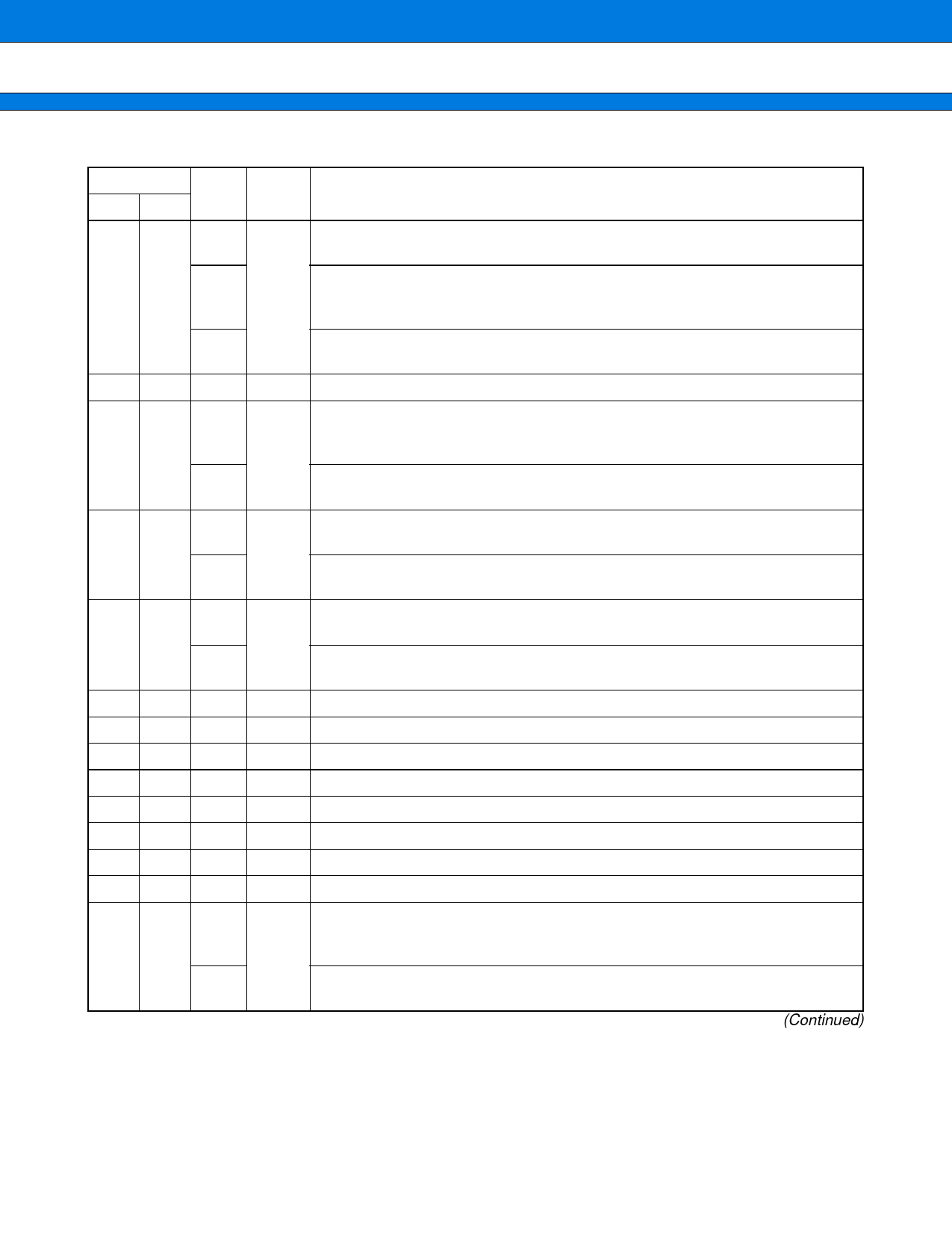
Pin no.
Pin Circuit
QFP LQFP name type
Description
PPG0
Output terminal of PPG timer 0.
This function becomes valid when output of PPG timer 0 is set to enabled.
External interrupt input terminal.
15 13 INT5 E When use the terminal as external input, output of PPG timer 0 is set to disabled,
and set the corresponding data direction resister (DDR) to input.
PG1
General purpose input/output port.
This function becomes valid when output of PPG temer 0 is set to disabled.
16 14 PG2 C General purpose input/output port.
UART2 data input terminal.
SIN2
When use the terminal as data input of UART2, set the corresponding data
20 18
D direction resister (DDR) to input.
PG3
General purpose input/output port.
This function is always valid.
SOT2
UART2 data output terminal.
This function becomes valid when data output of UART2 is set to enabled.
21 19
D
PG4
General purpose input/output port.
This function becomes valid when data output of UART2 is set to disabled.
SCK2
UART2 clock input/output terminal.
This function becomes valid when clock input/output of UART2 is set to enabled.
22 20
D
PG5
General purpose input/output port.
This function becomes valid when clock input/output of UART2 is set to disabled.
23 21 P40
C General purpose input/output port.
24 22 P41
C General purpose input/output port.
25 23 P42
C General purpose input/output port.
26 24 P43
C General purpose input/output port.
27 25 P44
C General purpose input/output port.
28 26 P45
C General purpose input/output port.
29 27 P46
C General purpose input/output port.
30 28 P47
C General purpose input/output port.
Analog input terminal of A/D converter.
AN11
This function becomes valid when set the corresponding AICR2 resister to
31 29
G analog input.
PE1
General purpose input/output port.
This function becomes valid when set the corresponding AICR2 resister to port.
(Continued)
7
Share Link: 