WF4M16-90DTC5A Просмотр технического описания (PDF) - White Electronic Designs => Micro Semi
Номер в каталоге
Компоненты Описание
производитель
WF4M16-90DTC5A Datasheet PDF : 11 Pages
| |||
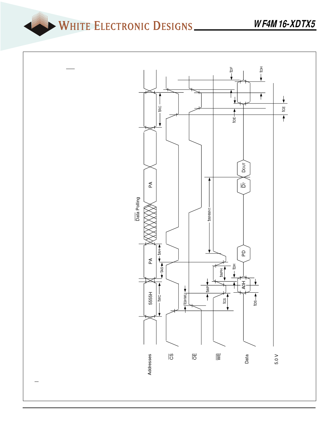
FIG. 4
WRITE/ERASE/PROGRAM
OPERATION, WE CONTROLLED
WF4M16-XDTX5
NOTES:
1. PA is the address of the memory location to be programmed.
2. PD is the data to be programmed at byte address.
3. D7 is the output of the complement of the data written to each chip.
4. DOUT is the output of the data written to the device.
5. Figure indicates last two bus cycles of four bus cycle sequence.
White Electronic Designs Corporation • (602) 437-1520 • www.whiteedc.com
6
Share Link: 