74LVC1G32GW Просмотр технического описания (PDF) - Panasonic Corporation
Номер в каталоге
Компоненты Описание
производитель
74LVC1G32GW Datasheet PDF : 14 Pages
| |||
Philips Semiconductors
Single 2-input OR gate
Product specification
74LVC1G32
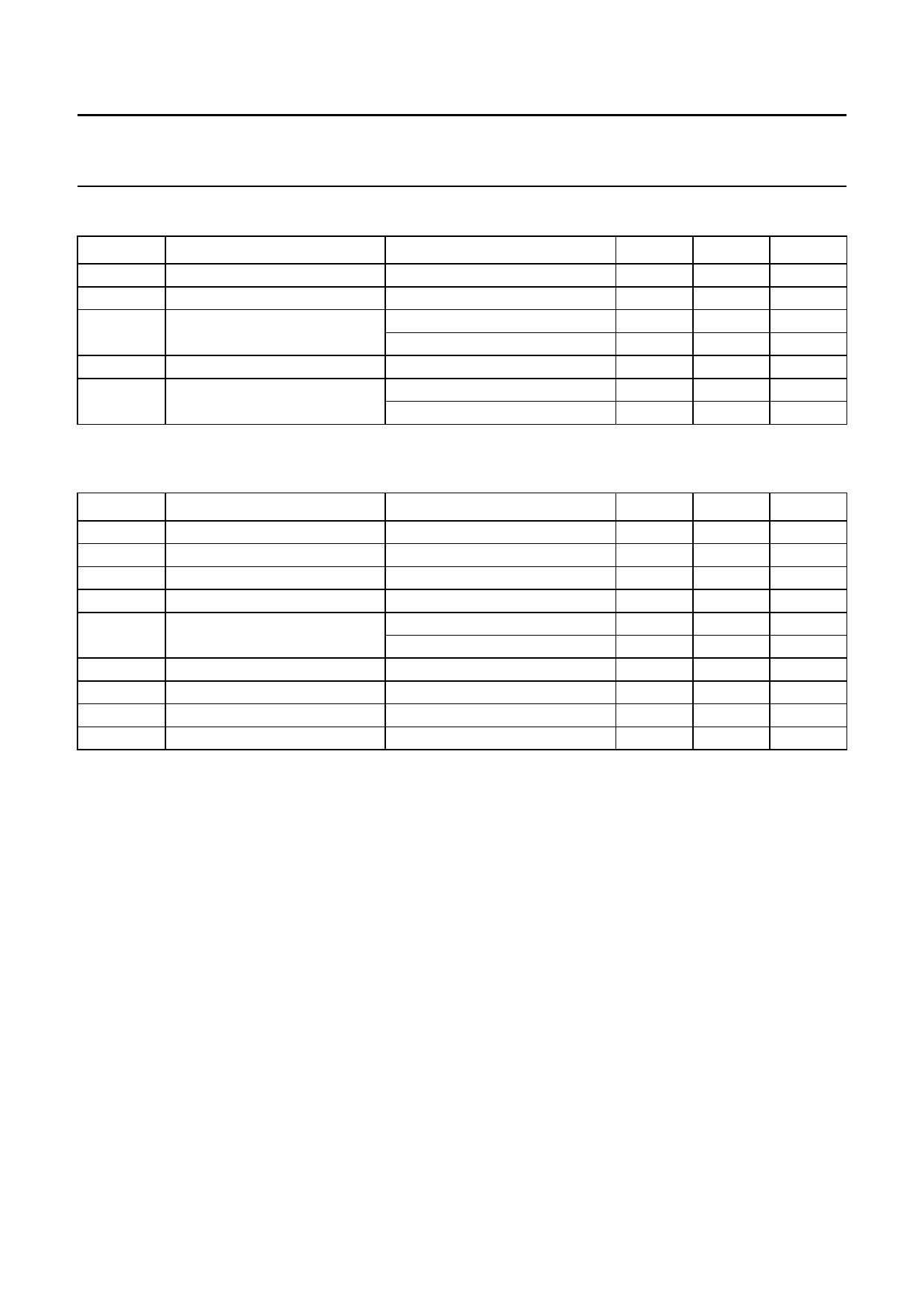
RECOMMENDED OPERATING CONDITIONS
SYMBOL
VCC
VI
VO
Tamb
tr, tf
PARAMETER
supply voltage
input voltage
output voltage
operating ambient temperature
input rise and fall times
CONDITIONS
active mode
VCC = 0 V; Power-down mode
VCC = 1.65 V to 2.7 V
VCC = 2.7 V to 5.5 V
MIN.
1.65
0
0
0
−40
0
0
MAX.
5.5
5.5
VCC
5.5
+125
20
10
UNIT
V
V
V
V
°C
ns/V
ns/V
LIMITING VALUES
In accordance with the Absolute Maximum Rating System (IEC 60134); voltages are referenced to GND (ground = 0 V).
SYMBOL
VCC
IIK
VI
IOK
VO
PARAMETER
supply voltage
input diode current
input voltage
output diode current
output voltage
IO
ICC, IGND
Tstg
Ptot
output diode current
VCC or GND current
storage temperature
power dissipation
CONDITIONS
MIN.
−0.5
VI < 0 V
note 1
−
−0.5
VO > VCC or VO < 0 V
active mode; notes 1 and 2
−
−0.5
Power-down mode; notes 1 and 2 −0.5
VO = 0 V to VCC
−
−
−65
Tamb = −40 °C to +125 °C
−
MAX.
UNIT
+6.5
V
−50
mA
+6.5
V
±50
mA
VCC + 0.5 V
+6.5
V
±50
mA
±100
mA
+150
°C
250
mW
Notes
1. The input and output voltage ratings may be exceeded if the input and output current ratings are observed.
2. When VCC = 0 V (Power-down mode), the output voltage can be 5.5 V in normal operation.
2004 Sep 15
5
Share Link: 