CAT5269 데이터 시트보기 (PDF) - Catalyst Semiconductor => Onsemi
부품명
상세내역
제조사
CAT5269
Catalyst Semiconductor => Onsemi
CAT5269 Datasheet PDF : 15 Pages
| |||
POWER UP TIMING (1)(2)
Symbol
Parameter
tPUR
Power-up to Read Operation
tPUW
Power-up to Write Operation
Max.
1
1
Units
ms
ms
CAT5269
XDCP TIMING
Symbol Parameter
tWRPO Wiper Response Time After Power Supply Stable
tWRL Wiper Response Time After Instruction Issued
Min Max Units
5
10 µs
5
10 µs
WRITE CYCLE LIMITS
Symbol
Parameter
tWR
Write Cycle Time
Max. Units
5
ms
The write cycle is the time from a valid stop condition of a write sequence to the end of the internal program/erase
cycle. During the write cycle, the bus interface circuits are disabled, SDA is allowed to remain high, and the device
does not respond to its slave address.
RELIABILITY CHARACTERISTICS
Symbol
NEND(1)
TDR(1)
VZAP(1)
ILTH(1)
Parameter
Endurance
Data Retention
ESD Susceptibility
Latch-Up
Min.
1,000,000
100
2000
100
Max.
Units
Cycles/Byte
Years
Volts
mA
Reference Test Method
MIL-STD-883, Test Method 1033
MIL-STD-883, Test Method 1008
MIL-STD-883, Test Method 3015
JEDEC Standard 17
Note:
(1) This parameter is tested initially and after a design or process change that affects the parameter.
(2) tPUR and tPUW are the delays required from the time VCC is stable until the specified operation can be initiated.
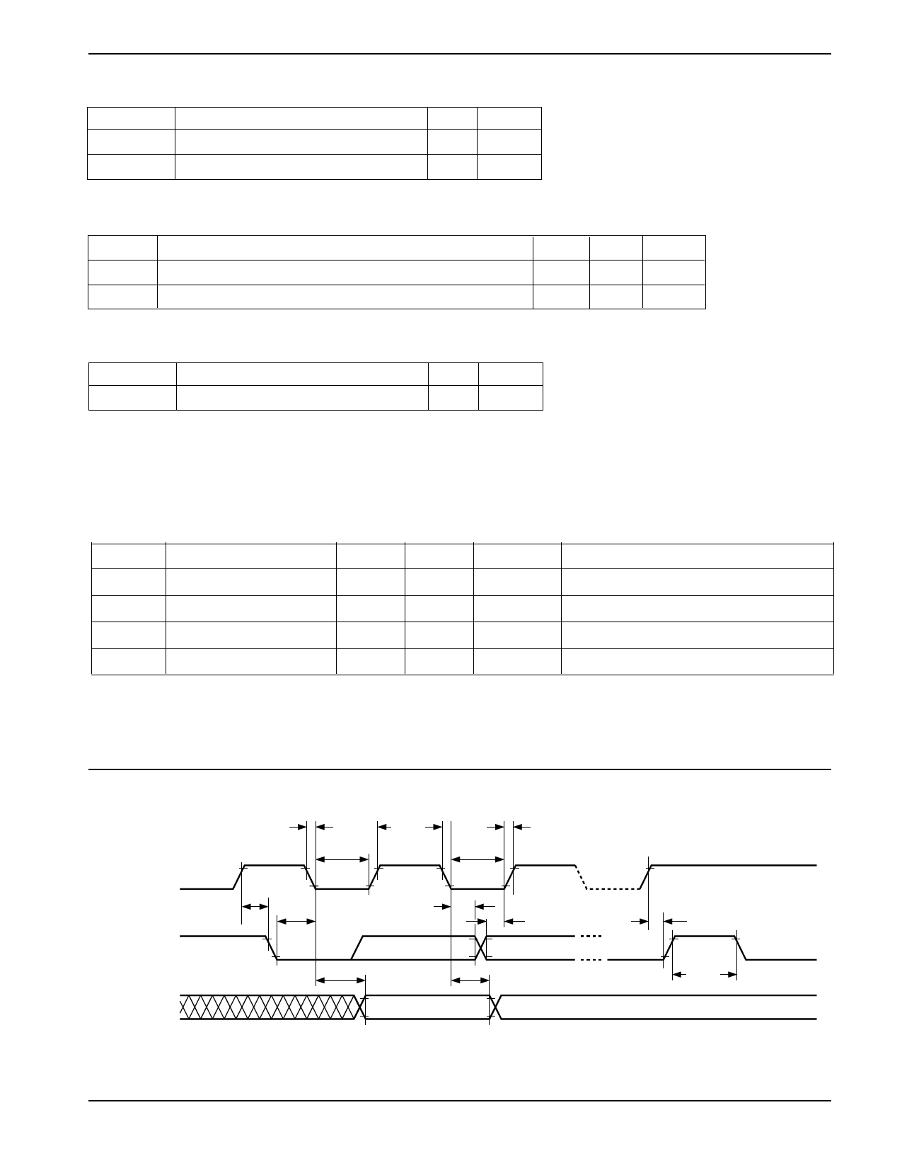
Figure 1. Bus Timing
tF
tHIGH
tR
tLOW
tLOW
SCL
tSU:STA
tHD:DAT
tHD:STA
tSU:DAT
SDA IN
SDA OUT
tAA
tDH
tSU:STO
tBUF
5
Document No. 2123, Rev. B
Share Link: 