ADP2164 데이터 시트보기 (PDF) - Analog Devices
부품명
상세내역
제조사
ADP2164 Datasheet PDF : 19 Pages
| |||
ADP2164
Data Sheet
APPLICATIONS INFORMATION
ADISIMPOWER DESIGN TOOL
The ADP2164 is supported by ADIsimPower design tool set.
ADIsimPower is a collection of tools that produce complete
power designs optimized for a specific design goal. The tools
enable the user to generate a full schematic, bill of materials,
and calculate performance in minutes. ADIsimPower can
optimize designs for cost, area, efficiency, and parts count
while taking into consideration the operating conditions and
limitations of the IC and all real external components. For
more information about ADIsimPower design tools, refer to
www.analog.com/ADIsimPower. The tool set is available from
this website, and users can also request an unpopulated board
through the tool.
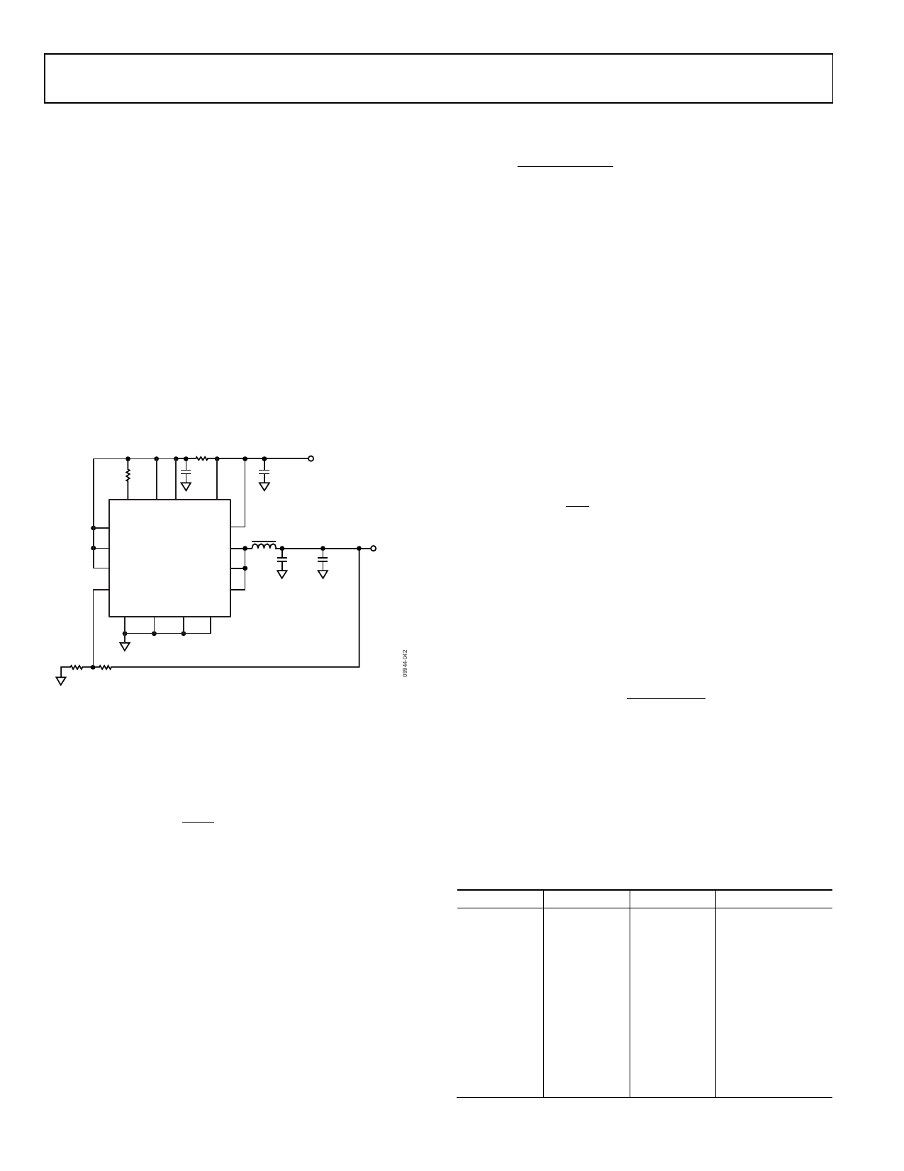
The typical application circuit for the ADP2164 is shown in
Figure 38.
R1
10Ω
R2
10kΩ
16 15 14
PGOOD EN VIN
C1
0.1µF
13
PVIN
CIN
47µF
X5R
10V
VIN
3.3V
1
SYNC
12
PVIN
2 RT ADP2164ACPZ SW 11
3
10
TRK
SW
4 FB
SW 9
L
0.8µH
COUT1
47µF
X5R
6.3V
COUT2
100µF
X5R
6.3V
VOUT
1.2V
4A
RBOT
10kΩ
GND
5
RTOP
10kΩ
PGND PGND PGND
6
7
8
L: MSS1048-801NL COILCRAFT
CIN: C3225X5R1A476M TDK
COUT1: C3225X5R0J476M TDK
COUT2: C3225X5R0J107M TDK
( ) L = VIN − VOUT × D
∆IL × fS
where:
VIN is the input voltage.
VOUT is the output voltage.
ΔIL is the inductor current ripple.
fS is the switching frequency.
D is the duty cycle (VOUT/VIN).
The ADP2164 uses slope compensation in the current control
loop to prevent subharmonic oscillations when the duty cycle
is larger than 50%. The internal slope compensation limits the
minimum inductor value.
The negative current limit (−1.3 A) also limits the minimum
inductor value. The inductor current ripple (ΔIL) calculated by
the selected inductor should not exceed 2.6 A.
The peak inductor current should be kept below the peak current
limit threshold and is calculated using the following equation:
I PEAK
=
IO
+
∆IL
2
Ensure that the rms current of the selected inductor is greater
than the maximum load current and that its saturation current
is greater than the peak current limit of the converter.
OUTPUT CAPACITOR SELECTION
The output capacitor value is determined by the output voltage
ripple, load step transient, and loop stability. The output ripple
is determined by the ESR and the capacitance.
Figure 38. Typical Application Circuit
OUTPUT VOLTAGE SELECTION
The output voltage of the adjustable version of the ADP2164 is
set by an external resistive voltage divider using the following
equation:
VOUT
= 0.6 × 1 +
RTOP
R BOT
To limit output voltage accuracy degradation due to FB bias
current (0.1 µA maximum) to less than 0.5% (maximum),
ensure that RBOT is less than 30 kΩ.
INDUCTOR SELECTION
The inductor value is determined by the operating frequency,
input voltage, output voltage, and ripple current. A small inductor
value provides larger inductor current ripple and fast transient
response but degrades efficiency; a large inductor value provides
small inductor current ripple and good efficiency but slows
transient response. For a reasonable trade-off between transient
response and efficiency, the inductor current ripple, ΔIL, is typically
set to one-third the maximum load current. The inductor value
is calculated using the following equation:
∆VOUT
=
∆I
L
×
ESR
+
8
1
× COUT
×
fS
The load step transient response depends on the inductor, the
output capacitor, and the current control loop.
The ADP2164 has integrated loop compensation for simple
power design. Table 5 and Table 6 show the recommended
values for inductors and capacitors for the ADP2164 based
on the input and output voltages for the part. X5R or X7R
dielectric ceramic capacitors are highly recommended.
Table 5. Recommended L and COUT Values at fS = 1.2 MHz
VIN (V)
VOUT (V)
L (µH)
COUT (µF)
3.3
1.0
0.8
100 + 100
3.3
1.2
0.8
100 + 47
3.3
1.5
1
100 + 47
3.3
1.8
1
100
3.3
2.5
1
47
5
1.0
0.8
100 + 100
5
1.2
0.8
100 + 47
5
1.5
1
100 + 47
5
1.8
1
100
5
2.5
1
47
5
3.3
1
47
Rev. C | Page 16 of 19
Share Link: 