ML9092-01TB 데이터 시트보기 (PDF) - LAPIS Semiconductor Co., Ltd.
부품명
상세내역
제조사
ML9092-01TB Datasheet PDF : 66 Pages
| |||
LAPIS Semiconductor
FEDL9092-01
ML9092-01/02/03/04
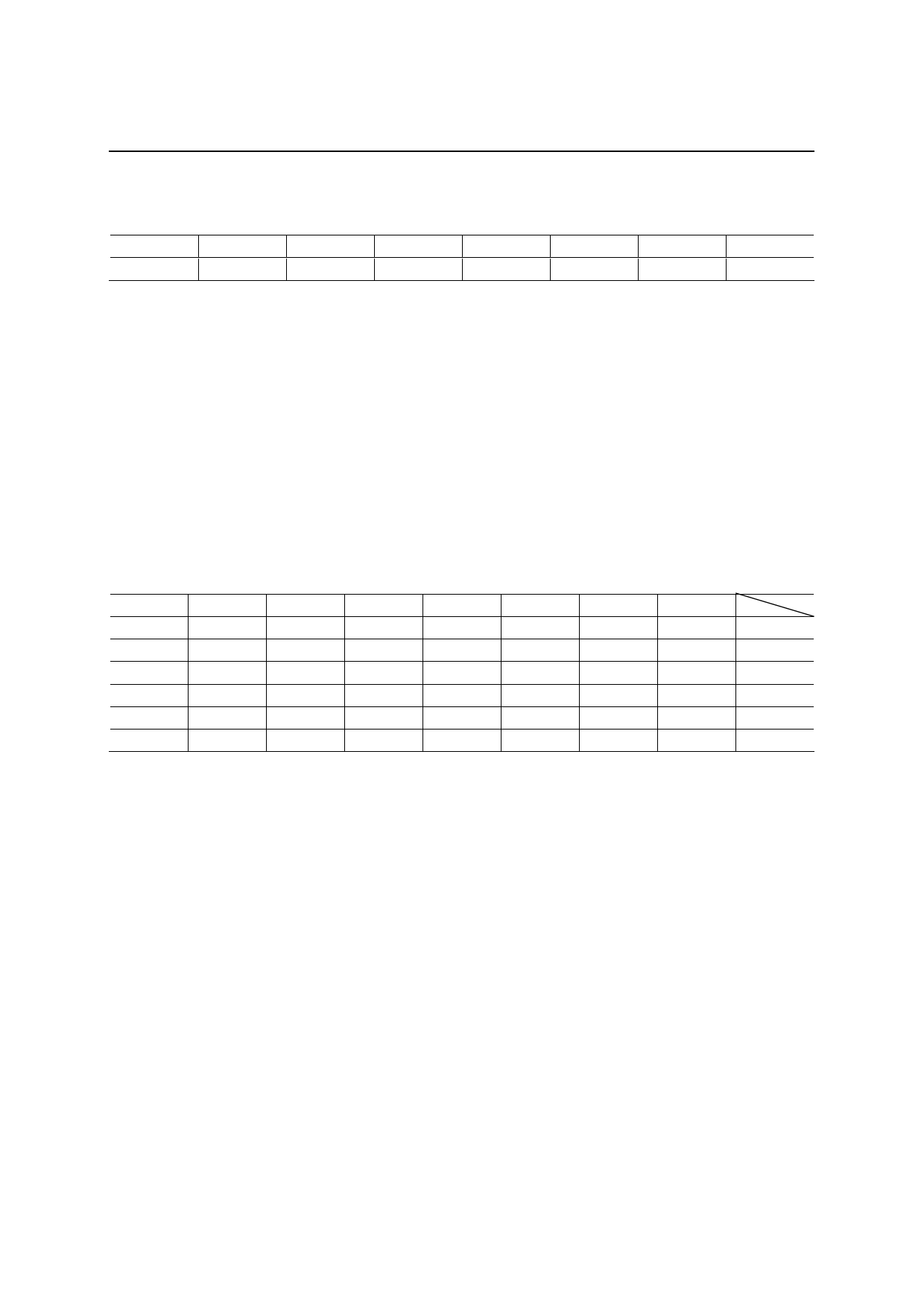
Key scan register (KR)—Read (for ML9092-02/03)
D7
D6
D5
D4
D3
D2
D1
D0
ST2
ST1
ST0
0
S3
S2
S1
S0
(1) D7 to D5 (ST2 to ST0) (Key scan read count display bits)
24-bit key scan data is divided into 6 groups and read. The read count is indicated by bits ST2 to ST0.
Every time key scan data is read, these bits are automatically incremented over the range of “000” to “101”. After
counting to “101”, this counter is reset to “000” and then again incremented from “000”, thereafter repeating this
cycle. If the CS signal is risen up during the cycle of counting, the scan read counter bits are returned to “000”.
If the RESET pin is pulled to a “L” level, these bits are reset to “0”.
(2) D3 to D0 (S3 to S0) (Key scan read data bits)
These bits are read as 24-bit serial data that expresses the key switch status (1 = ON, 0 = OFF). Data is divided into
6 groups and read. (For the read order, refer to the description below.) The read count is indicated by bits ST2 to
ST0.
The correspondence between the scan read count data, key scan data and key matrix switches is shown below.
If the RESET pin is pulled to a “L” level, these bits are reset to “0”.
ST2
ST1
ST0
0
0
0
0
0
1
0
1
0
0
1
1
1
0
0
1
0
1
S4
S3
S2
S1
S0
0
SW03
SW02
SW01
SW00
R0
0
SW13
SW12
SW11
SW10
R1
0
SW23
SW22
SW21
SW20
R2
0
SW33
SW32
SW31
SW30
R3
0
SW43
SW42
SW41
SW40
R4
0
SW53
SW52
SW51
SW50
R5
Note: SW00 to SW53 indicate the corresponding switches in Figure 2.
41/66
Share Link: 