IR51H310 데이터 시트보기 (PDF) - International Rectifier
부품명
상세내역
제조사
IR51H310 Datasheet PDF : 6 Pages
| |||
IR51H310
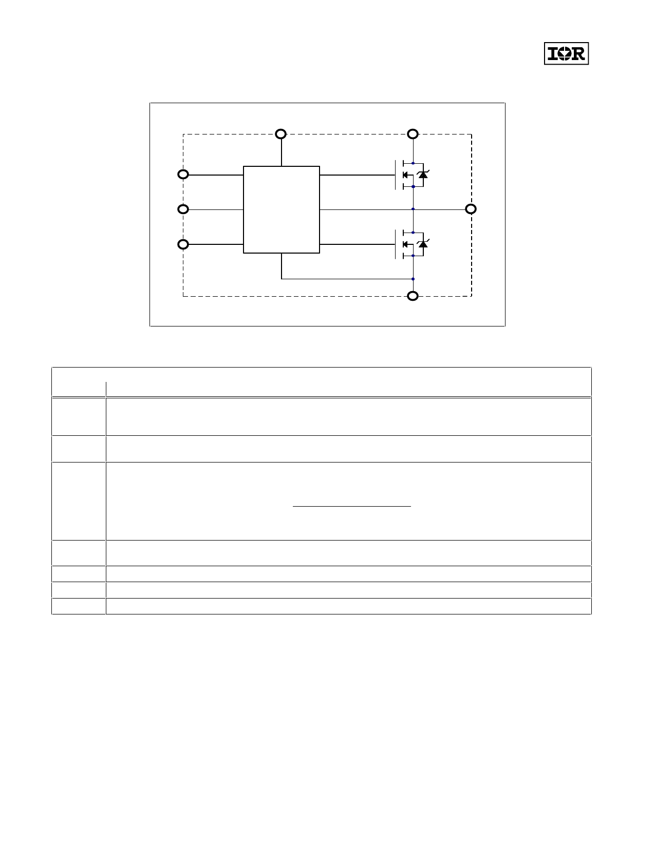
Functional Block Diagram
1
VCC
2
RT
3
CT
VB
6
IR 2 1 5 1
VIN
9
IR F C 3 1 0
7
VO
IR F C 3 1 0
4
COM
Lead Definitions
Symbol
VCC
RT
CT
Lead
Description
Logic and internal gate drive supply voltage. An internal zener clamp diode at 15.6 V nominal is
included to allow the VCC to be current fed directly from VIN typically by means of a high value
resistor.
Oscillator timing resistor input; a resistor is connected from RT to CT. RT is out of phase with
the half-bridge output (VO).
Oscillator timing capacitor output; a capacitor is connected from CT to COM in order to program
the oscillator frequency according to the following equation:
f=
1
1. 4 × (RT + 75Ω) × CT
where 75Ω is the effective impedance of the RT output stage.
VB
High side gate drive floating supply. For bootstrap operation a high voltage fast recovery diode is
needed to feed from VCC to VB.
VIN
High voltage supply.
VO
Half-bridge output.
COM Logic and low side of half-bridge return.
Share Link: 