HIP6018BCBZ-T 데이터 시트보기 (PDF) - Renesas Electronics
부품명
상세내역
제조사
HIP6018BCBZ-T Datasheet PDF : 15 Pages
| |||
HIP6018B
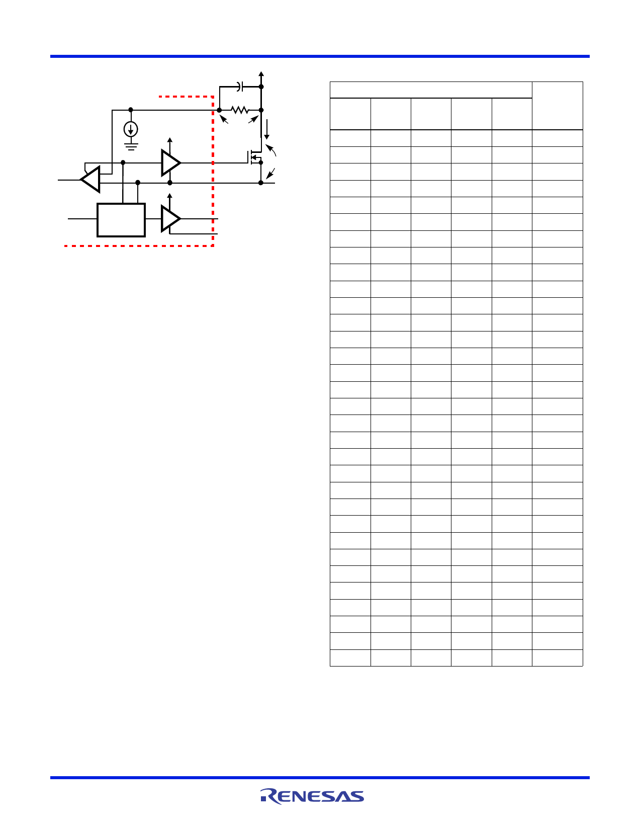
OVER-CURRENT TRIP: VDS > VSET
(iD • rDS(ON) > IOCSET • ROCSET)
OCSET
IOCSET
200A
VCC
DRIVE
OC1
+
-
OVER-
CURRENT1
PWM
HIP6018B
GATE
CONTROL
UGATE
PHASE
VCC
LGATE
PGND
VIN = +5V
ROCSET
VSET +
ID
+
VDS
VPHASE = VIN - VDS
VOCSET = VIN - VSET
FIGURE 9. OVER-CURRENT DETECTION
The OC trip point varies with MOSFET’s temperature. To avoid
over-current tripping in the normal operating load range,
determine the ROCSET resistor from the equation above with:
1. The maximum rDS(ON) at the highest junction temperature.
2. The minimum IOCSET from the specification table.
3. Determine IPEAK for IPEAK > IOUT(MAX) + (I)/2,
where I is the output inductor ripple current.
For an equation for the output inductor ripple current see the
section under component guidelines titled ‘Output Inductor
Selection’.
OUT1 Voltage Program
The output voltage of the PWM converter is programmed to
discrete levels between 1.3VDC and 3.5VDC. This output is
designed to supply the microprocessor core voltage. The
voltage identification (VID) pins program an internal voltage
reference (DACOUT) through a TTL-compatible 5-bit digital-
to-analog converter. The level of DACOUT also sets the
PGOOD and OVP thresholds. Table 1 specifies the DACOUT
voltage for the different combinations of connections on the
VID pins. The VID pins can be left open for a logic 1 input,
because they are internally pulled up to +5V by a 10A
(typically) current source. Changing the VID inputs during
operation is not recommended. The sudden change in the
resulting reference voltage could toggle the PGOOD signal
and exercise the over-voltage protection.
The ‘11111’ VID pin combination resulting in an INHIBIT
disables the IC and the open-collector at the PGOOD pin.
VID4
TABLE 1. VOUT1 VOLTAGE PROGRAM
PIN NAME
VID3
VID2
VID1
VID0
NOMINAL
OUT1
VOLTAGE
DACOUT
0
1
1
1
1
1.30
0
1
1
1
0
1.35
0
1
1
0
1
1.40
0
1
1
0
0
1.45
0
1
0
1
1
1.50
0
1
0
1
0
1.55
0
1
0
0
1
1.60
0
1
0
0
0
1.65
0
0
1
1
1
1.70
0
0
1
1
0
1.75
0
0
1
0
1
1.80
0
0
1
0
0
1.85
0
0
0
1
1
1.90
0
0
0
1
0
1.95
0
0
0
0
1
2.00
0
0
0
0
0
2.05
1
1
1
1
1
INHIBIT
1
1
1
1
0
2.1
1
1
1
0
1
2.2
1
1
1
0
0
2.3
1
1
0
1
1
2.4
1
1
0
1
0
2.5
1
1
0
0
1
2.6
1
1
0
0
0
2.7
1
0
1
1
1
2.8
1
0
1
1
0
2.9
1
0
1
0
1
3.0
1
0
1
0
0
3.1
1
0
0
1
1
3.2
1
0
0
1
0
3.3
1
0
0
0
1
3.4
1
0
0
0
0
3.5
NOTE: 0 = connected to GND or VSS, 1 = open or connected to 5V
through pull-up resistors.
FN4586 Rev 3.00
April 1, 2005
Page 9 of 15
Share Link: 