ICX039DNA 데이터 시트보기 (PDF) - Sony Semiconductor
부품명
상세내역
제조사
ICX039DNA Datasheet PDF : 21 Pages
| |||
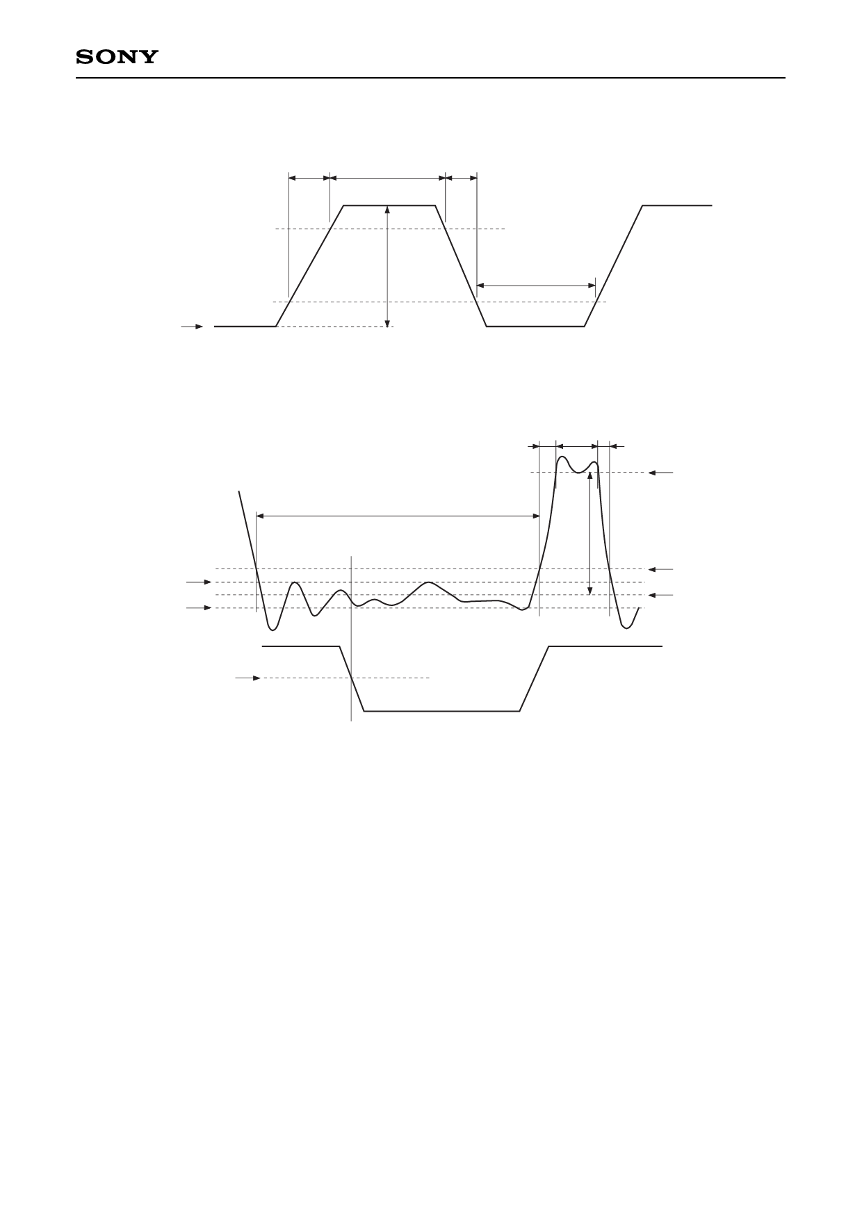
(3) Horizontal transfer clock waveform
tr
twh
tf
90%
10%
VHL
VφH
twl
ICX039DNA
(4) Reset gate clock waveform
RG waveform
VRGLH
VRGLL
Hφ1 waveform
+2.5V
twl
Point A
tr
twh
tf
VRGH
VφRG
VRGL + 0.5V
VRGL
VRGLH is the maximum value and VRGLL is the minimum value of the coupling waveform during the period from
Point A in the above diagram until the rising edge of RG. In addition, VRGL is the average value of VRGLH and
VRGLL.
VRGL = (VRGLH + VRGLL)/2
Assuming VRGH is the minimum value during the period twh, then:
VφRG = VRGH – VRGL
–8–
Share Link: 