CS5166 데이터 시트보기 (PDF) - ON Semiconductor
부품명
상세내역
제조사
CS5166 Datasheet PDF : 25 Pages
| |||
CS5166
M 10.0 μs
Trace 1− Regulator Output Voltage (5.0 V/div.)
Trace 2− Inductor Switching Node (5.0 V/div.)
Figure 13. Demonstration Board Enable Startup
Waveforms
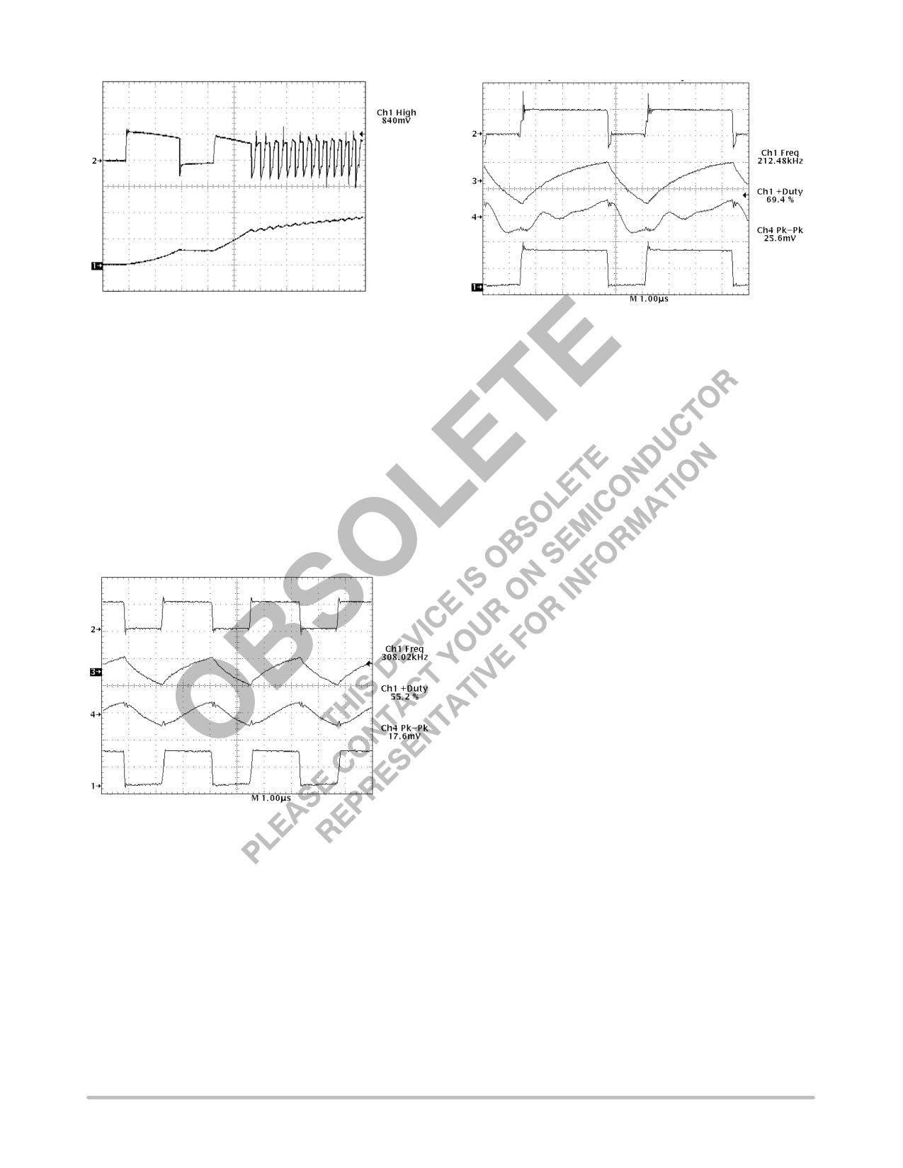
Normal Operation
During normal operation, switch off time is constant and
set by the COFF capacitor. Switch on time is adjusted by the
V2 control loop to maintain regulation. This results in
changes in regulator switching frequency, duty cycle, and
output ripple in response to changes in load and line. Output
voltage ripple will be determined by inductor ripple current
working and the ESR of the output capacitors (see Figures
14 and 15).
Trace 1− GATE(H) (10 V/div.)
Trace 2− Inductor Switching Node (5.0 V/div.)
Trace 3− Output Inductor Ripple Current (2.0 A/div.)
Trace 4− VOUT ripple (20 mV/div.)
Figure 14. Normal Operation Showing Output
Inductor Ripple Current and Output Voltage
Ripple, 0.5 A Load, VOUT = +2.825 V (DAC = 10111)
Trace 1− GATE(H) (10 V/div.)
Trace 2− Inductor Switching Node (5.0 V/div.)
Trace 3− Output Inductor Ripple Current (2.0 A/div.)
Trace 4− VOUT ripple (20 mV/div.)
Figure 15. Normal Operation Showing
Output Inductor Ripple Current and Output
Voltage Ripple, ILOAD = 14 A, VOUT = +2.825 V
(DAC = 10111)
Transient Response
The CS5166 V2 control loop’s 150 ns reaction time
provides unprecedented transient response to changes in
input voltage or output current. Pulse by pulse adjustment of
duty cycle is provided to quickly ramp the inductor current
to the required level. Since the inductor current cannot be
changed instantaneously, regulation is maintained by the
output capacitor(s) during the time required to slew the
inductor current.
Overall load transient response is further improved
through a feature called “Adaptive Voltage Positioning”.
This technique pre−positions the output capacitors voltage
to reduce total output voltage excursions during changes in
load.
Holding tolerance to 1.0% allows the error amplifiers
reference voltage to be targeted +25 mV high without
compromising DC accuracy. A “Droop Resistor”,
implemented through a PC board trace, connects the Error
Amps feedback pin (VFB) to the output capacitors and load
and carries the output current. With no load, there is no DC
drop across this resistor, producing an output voltage
tracking the Error amps, including the +25 mV offset. When
the full load current is delivered, an 50 mV drop is developed
across this resistor. This results in output voltage being
offset −25 mV low.
The result of Adaptive Voltage Positioning is that
additional margin is provided for a load transient before
http://onsemi.com
12
Share Link: 