A2588 데이터 시트보기 (PDF) - Allegro MicroSystems
부품명
상세내역
제조사
A2588 Datasheet PDF : 12 Pages
| |||
2580, 2585, AND 2588
8-CHANNEL
SOURCE DRIVERS
UDN2585A and A2585SLW
ELECTRICAL CHARACTERISTICS at TA = +25°C, VS = 0 V, VEE = -20 V (unless otherwise noted).
Characteristic
Output Leakage
Current
Output Sustaining
Voltage
Output Saturation
Voltage
Input Current
Input Voltage
Clamp Diode
Leakage Current
Symbol
ICEX
VCE(SUS)
VCE(SAT)
IIN(ON)
VIN(ON)
VIN(OFF)
IR
Test Conditions
VlN = -0.5 V, VOUT = VEE = -25 V
VlN = -0.4 V, VOUT = VEE = -25 V, TA = 70°C
VlN = -0.4 V, IOUT = -25 mA, Note 1
VlN = -4.6 V, IOUT = -60 mA
VlN = -4.6 V, IOUT = -120 mA
VlN = -4.6 V, IOUT = -120 mA
VlN = -14.6 V, IOUT = -120 mA
IOUT = -120 mA, VCE ≤1.2 V, Note 3
IOUT = -100 µA, TA = 70°C
VR = 25 V, TA = 70°C
Min.
—
—
15
—
—
—
—
—
-0.4
—
Limits
Max.
50
100
—
1.1
1.2
-1.6
-5.0
-4.6
—
50
Units
µA
µA
V
V
V
mA
mA
V
V
µA
Clamp Diode
VF
IF = 120 mA
Forward Voltage
—
2.0
V
Input Capacitance
CIN
Turn-On Delay
tPHL
Turn-Off Delay
tPLH
0.5 EIN to 0.5 EOUT
0.5 EIN to 0.5 EOUT
—
25
pF
—
5.0
µs
—
5.0
µs
NOTES: 1. Pulsed test, tp ≤ 300 µs, duty cycle ≤ 2%.
2. Negative current is defined as coming out of the specified device pin.
3. The VIN(ON) voltage limit guarantees a minimum output source current per the specified conditions.
4. The substrate must always be tied to the most negative point and must be at least 4.0 V below VS.
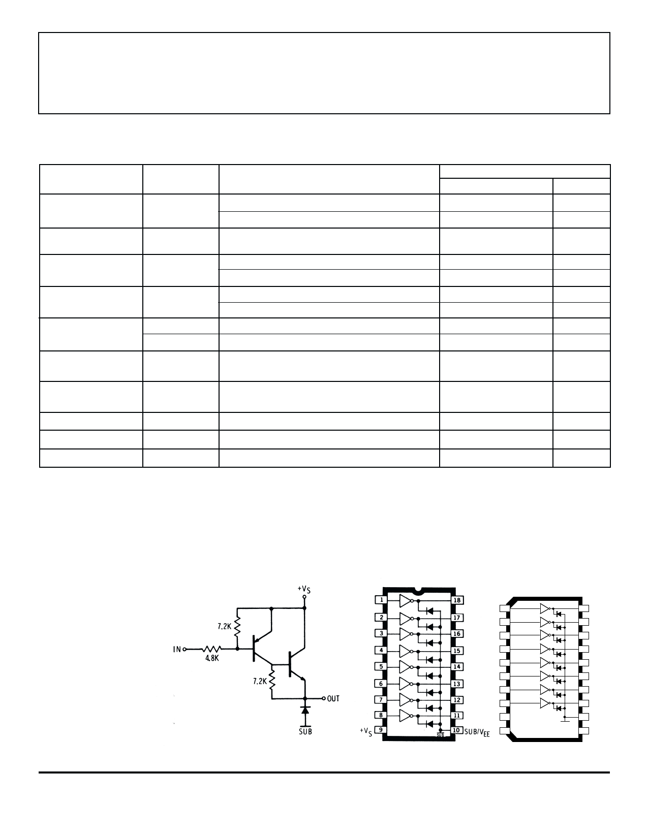
PARTIAL SCHEMATIC
UDN2585A
A2585SLW
www.allegromicro.com
Dwg. No. A-11,360
1
2
3
4
5
6
7
8
+VS 9
10 NC
Dwg. No. A-11,359
20
19
18
17
16
15
14
13
12
SUB
NC 11
SUB/VEE
Dwg. PP-064
5
Share Link: 