BFG25AW-X 데이터 시트보기 (PDF) - Philips Electronics
부품명
상세내역
제조사
BFG25AW-X Datasheet PDF : 16 Pages
| |||
Philips Semiconductors
Product specification
NPN 5 GHz wideband transistors
BFG25AW; BFG25AW/X
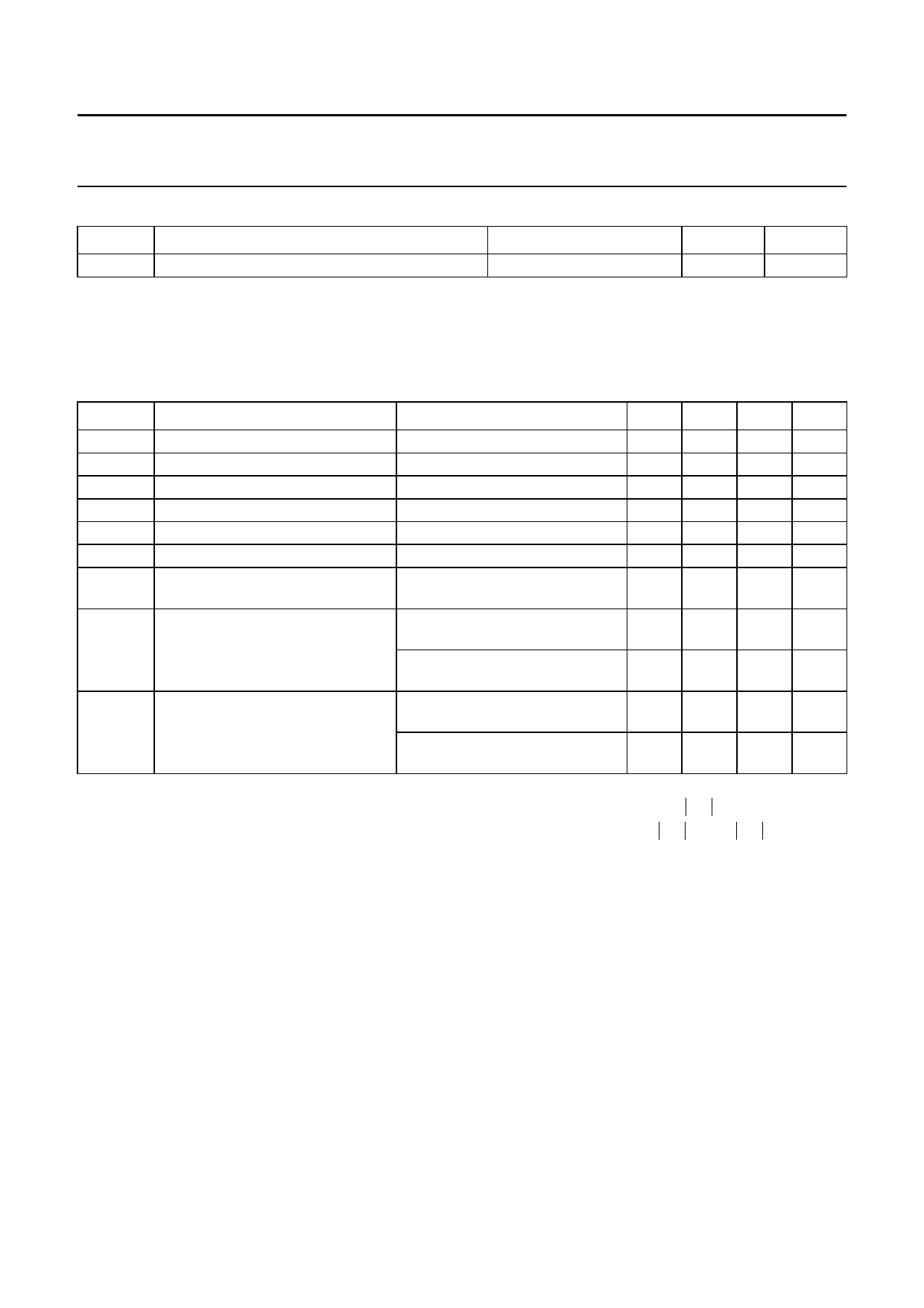
THERMAL CHARACTERISTICS
SYMBOL
PARAMETER
CONDITIONS
Rth j-s
thermal resistance from junction to soldering point Ts ≤ 85 °C; note 1
Note
1. Ts is the temperature at the soldering point of the collector pin.
VALUE
180
UNIT
K/W
CHARACTERISTICS
Tj = 25 °C unless otherwise specified.
SYMBOL
PARAMETER
CONDITIONS
MIN. TYP. MAX. UNIT
V(BR)CBO
V(BR)CEO
V(BR)EBO
collector-base breakdown voltage IC = 100 µA; IE = 0
collector-emitter breakdown voltage IC = 1 mA; IB = 0
emitter-base breakdown voltage IE = 100 µA; IC = 0
−
−
8
V
−
−
5
V
−
−
2
V
ICBO
collector leakage current
open emitter; VCB = 5 V; IE = 0 −
−
50
nA
hFE
DC current gain
Cre
feedback capacitance
IC = 0.5 mA; VCE = 1 V
IC = 0; VCE = 1 V; f = 1 MHz
50
80
200
−
0.2 0.3 pF
fT
transition frequency
IC = 1 mA; VCE = 1 V; f = 1 GHz; 3.5 5
−
GHz
Tamb = 25 °C
GUM
maximum unilateral power gain;
note 1
IC = 0.5 mA; VCE = 1 V;
f = 1 GHz; Tamb = 25 °C
−
16
−
dB
IC = 0.5 mA; VCE = 1 V;
f = 2 GHz; Tamb = 25 °C
−
8
−
dB
F
noise figure
Γs = Γopt; IC = 0.5 mA; VCE = 1 V; −
1.9 −
dB
f = 1 GHz
Γs = Γopt; IC = 1 mA; VCE = 1 V; −
2
dB
f = 1 GHz
Note
1. GUM is the maximum unilateral power gain, assuming S12 is zero. GUM
=
10
log --(--1-----–------S----1---1----S2---)-2---1(---1-2----–------S----2--2-----2---)-
dB.
1998 Sep 23
3
Share Link: 