LTC1340 데이터 시트보기 (PDF) - Linear Technology
부품명
상세내역
제조사
LTC1340 Datasheet PDF : 8 Pages
| |||
LTC1340
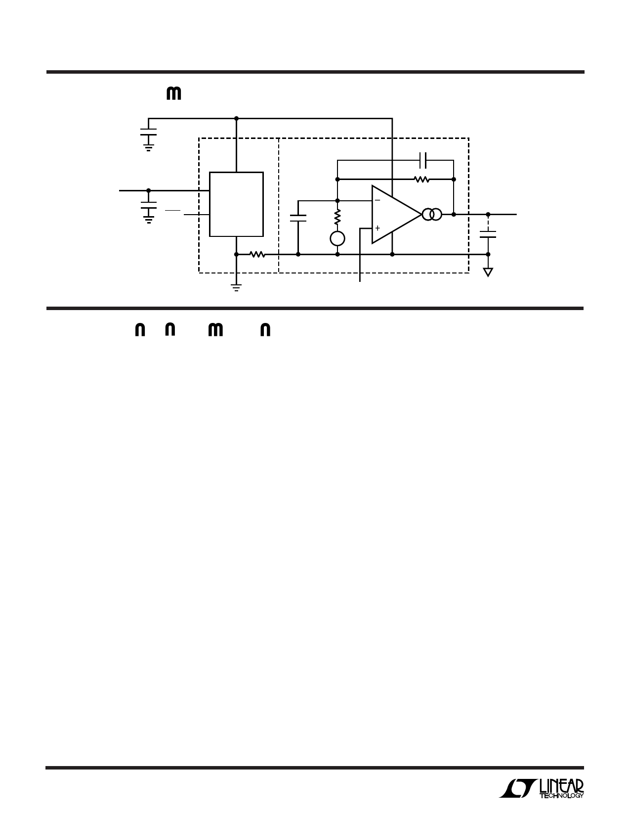
BLOCK DIAGRAM
CCP
0.1µF
(EXTERNAL)
PGND
VCC
0.1µF
SHDN
CP
LTC1340
AVCC
47.9pF
DOUBLER
CHARGE
PUMP WITH
INTERNAL
FLYING
CAPACITOR
50Ω
1.5M
–
62.3pF 1.15M +
VS
0.62V
+
–
PGND
IN
OUT
±20µA
COUT
(EXTERNAL)
AGND
1340 BD
APPLICATIONS INFORMATION
Overview
The LTC1340 is a monolithic IC that combines a charge
pump and a low noise amplifier to provide a 0V to 5V swing
to drive a varactor diode-based PLL system from a single
3V supply. Traditional PLL frequency synthesizers used in
cellular phones and other portable RF systems use varactor
diodes as the voltage variable element in the VCO. Typical
varactor diodes require at least 4V of control voltage swing
to obtain their full range of capacitance adjustment. Newer
battery-powered systems, operating from low voltage
power supplies, have trouble providing this bias voltage
without an additional step-up circuit.
The LTC1340 design provides a 5V signal swing suitable
for biasing such a varactor diode when powered from a 3V
or higher voltage supply. The internal op amp and feed-
back network with built-in offset provide a gain of 2.3 so
that a 0.35V to 2.5V swing at the noninverting input
provides a 0V to 5V swing at the output. The onboard
charge pump provides the boosted voltage necessary to
drive the varactor and requires only a single 0.1µF output
filter capacitor to complete the boost circuit. The amplifier
requires one capacitor (typically 1nF) at its output to set
amplifier noise bandwidth and to ensure amplifier stabil-
ity. The performance characteristics of the LTC1340 are
designed to meet the requirements of GSM and similar
cellular phone transceivers without requiring additional
circuitry. The LTC1340’s high level of functional integra-
tion allows it to replace several power supply and regulator
components in a typical PLL synthesizer. This results in
significant space and complexity savings.
Charge Pump
The LTC1340 features a self-contained doubling charge
pump with internal flying capacitors. The charge pump
refreshes the output on each phase of the internal 2MHz
clock, giving an effective 4MHz switching frequency. An
external 0.1µF capacitor at the CP pin acts as a charge
reservoir and provides filtering to minimize clock
feedthrough to the amplifier section. The CP pin can be
connected directly to the amplifier power supply at AVCC.
In addition, it can be filtered with an RC or LC network prior
to its connection to AVCC. The LTC1340 minimizes inter-
action between the charge pump and the amplifier through
careful internal shielding.
Amplifier
The LTC1340 includes an internal gm amplifier with an on-
chip feedback network to amplify the input signal to the
gained output level. The amplifier requires an external
capacitor from its output to AGND to provide closed-loop
stability, noise bandwidth limiting and to further reduce
charge pump feedthrough. The – 3dB signal bandwidth of
the amplifier is given by the following equation:
BW–3dB = gm/(2π)( COUT)(AV)
6
Share Link: 