MIKROE-1435 데이터 시트보기 (PDF) - Unspecified
부품명
상세내역
제조사
MIKROE-1435 Datasheet PDF : 2 Pages
| |||
5. ccRF click™ Board Schematic
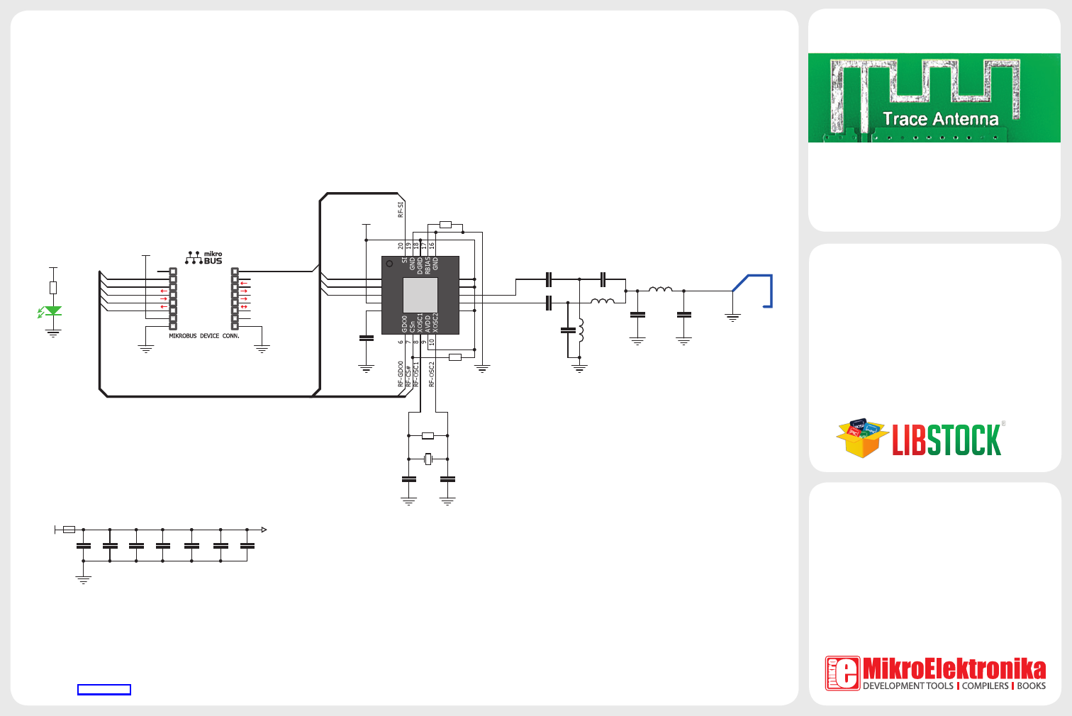
6. PCB Trace Antenna
VCC3.3
R2
2K2
LD1
VCC3.3
RF-GDO0
RF-CS#
RF-SCLK
RF-SO
RF-SI
AN
RST
CS
SCK
MISO
MOSI
+3.3V
GND
PWM
INT
TX
RX
SCL
SDA
+5V
GND
VCC-RF
R1 56K
RF-GDO2
RF-SCLK
RF-SO
RF-GDO2
U1
1
2
3
4
5
SCLK
SO
GDO2
DVDD
DCPL
CC2500
GND
AVDD 15
AVDD 14
RF_N 13
RF_P 12
AVDD 11
C7
100nF
R3 10K
FP1
VCC3.3
C8
10uF
C9
C10
C11
100nF 100nF 220pF
VCC-RF
C12
C13
C14
220pF 100nF 100nF
R4 1M
X1
26MHz
C15
22pF
C16
22pF
C1 100pF
C2 1pF
C3 100pF
C6
1pF
L2 1.2nH
L3
1.2nH
L1 1.2nH
A1
IFA_2.4GHz
ANT
C4
1.8pF
C5
1.5pF
Board features PCB trace antenna, designed
for the 2400-2483.5 MHz frequency band.
Maximum device range is up to 20 meters in
open space.
7. Code Examples
Once you have done all the necessary
preparations, it’s time to get your click™
board up and running. We have provided
the examples for mikroC™, mikroBasic™ and
mikroPascal™ compilers on our Libstock
website. Just download them and you are
ready to start.
.com
8. Support
MikroElektronika offers Free Tech Support
(www.mikroe.com/esupport) until the end
of product lifetime, so if something goes
wrong, we are ready and willing to help!
MikroElektronika assumes no responsibility or liability for any errors or inaccuracies that may appear in the present document.
Specification and information contained in the present schematic are subject to change at any time without notice. Copyright © 2013 MikroElektronika. All rights reserved.
Share Link: 