MK2727S 데이터 시트보기 (PDF) - Integrated Circuit Systems
부품명
상세내역
제조사
MK2727S Datasheet PDF : 4 Pages
| |||
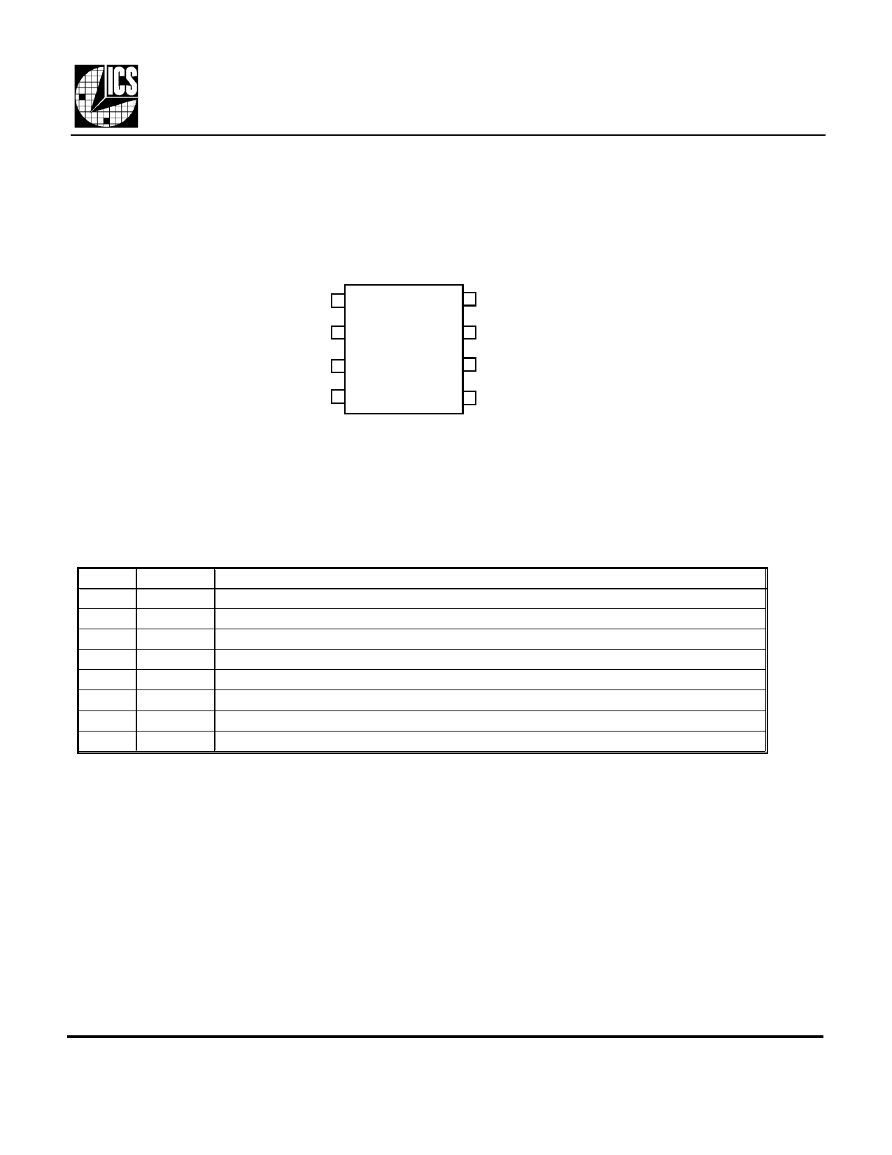
Pin Assignment
MK2727
Low Cost 27 MHz VCXO
MK2727
X1 1
VDD 2
VIN 3
GND 4
8 X2
7 GND
6 VDD
5 CLK
8 pin (150 mil) SOIC
Pin Descriptions
Number
1
2
3
4
5
6
7
8
Name
X1
VDD
VIN
GND
CLK
VDD
GND
X2
Description
Crystal connection. Connect to a pullable 13.5 MHz crystal.
VDD. Connect to +5V.
Voltage input to VCXO. Zero to 3V analog input which controls the frequency of the VCXO.
Connect to ground.
27 MHz clock output.
VDD. Connect to +5V.
Connect to ground.
Crystal connection. Connect to a pullable 13.5 MHz crystal.
MDS 2727 B
2
Revision 111600
Printed 11/16/00
Integrated Circuit Systems, Inc.•525 Race Street•San Jose•CA•95126•(408)295-9800tel•www.icst.com
Share Link: 