ISPPAC-CLK5320S-01T64I 데이터 시트보기 (PDF) - Lattice Semiconductor
부품명
상세내역
제조사
ISPPAC-CLK5320S-01T64I
Lattice Semiconductor
ISPPAC-CLK5320S-01T64I Datasheet PDF : 56 Pages
| |||
Lattice Semiconductor
ispClock5300S Family Data Sheet
General Description
The ispClock5300S is an in-system-programmable zero delay universal fan-out buffer for use in clock distribution
applications. The ispClock5312S, the first member of the ispClock5300S family, provides up to 12 single-ended
ultra low skew outputs. Each pair of outputs may be independently configured to support separate I/O standards
(LVTTL, LVCMOS -3.3V, 2.5V, 1.8, SSTL, HSTL) and output frequency. In addition, each output provides indepen-
dent programmable control of termination, slew-rate, and timing skew. All configuration information is stored on-
chip in non-volatile E2CMOS® memory.
The ispClock5300S devices provide extremely low propagation delay (zero-delay) from input to output using the
on-chip low jitter high-performance PLL. A set of three programmable 5-bit counters can be used to generate three
frequencies derived from the PLL clock. These counters are programmable in powers of 2 only (1, 2, 4, 8, 16, 32).
The clock output from any of the V-dividers can then be routed to any clock output pin through the output routing
matrix. The output routing matrix, in addition, also enables routing of reference clock inputs directly to any output.
The ispClock5300S device can be configured to operate in four modes: zero delay buffer mode, dual non-zero
delay buffer mode, non-zero delay buffer mode with output dividers, and combined zero-delay and non-zero delay
buffer mode.
The core functions of all members of the ispClock5300S family are identical. Table 1 summarizes the
ispClock5300S device family.
Table 1. ispClock5300S Family
Device
ispClock5320S
ispClock5316S
ispClock5312S
ispClock5308S
ispClock5304S
Number of Programmable
Clock Inputs
1 Differential, 2 Single-Ended
1 Differential, 2 Single-Ended
1 Differential, 2 Single-Ended
1 Differential, 2 Single-Ended
1 Differential, 2 Single-Ended
Number of Programmable
Single-Ended Outputs
20
16
12
8
4
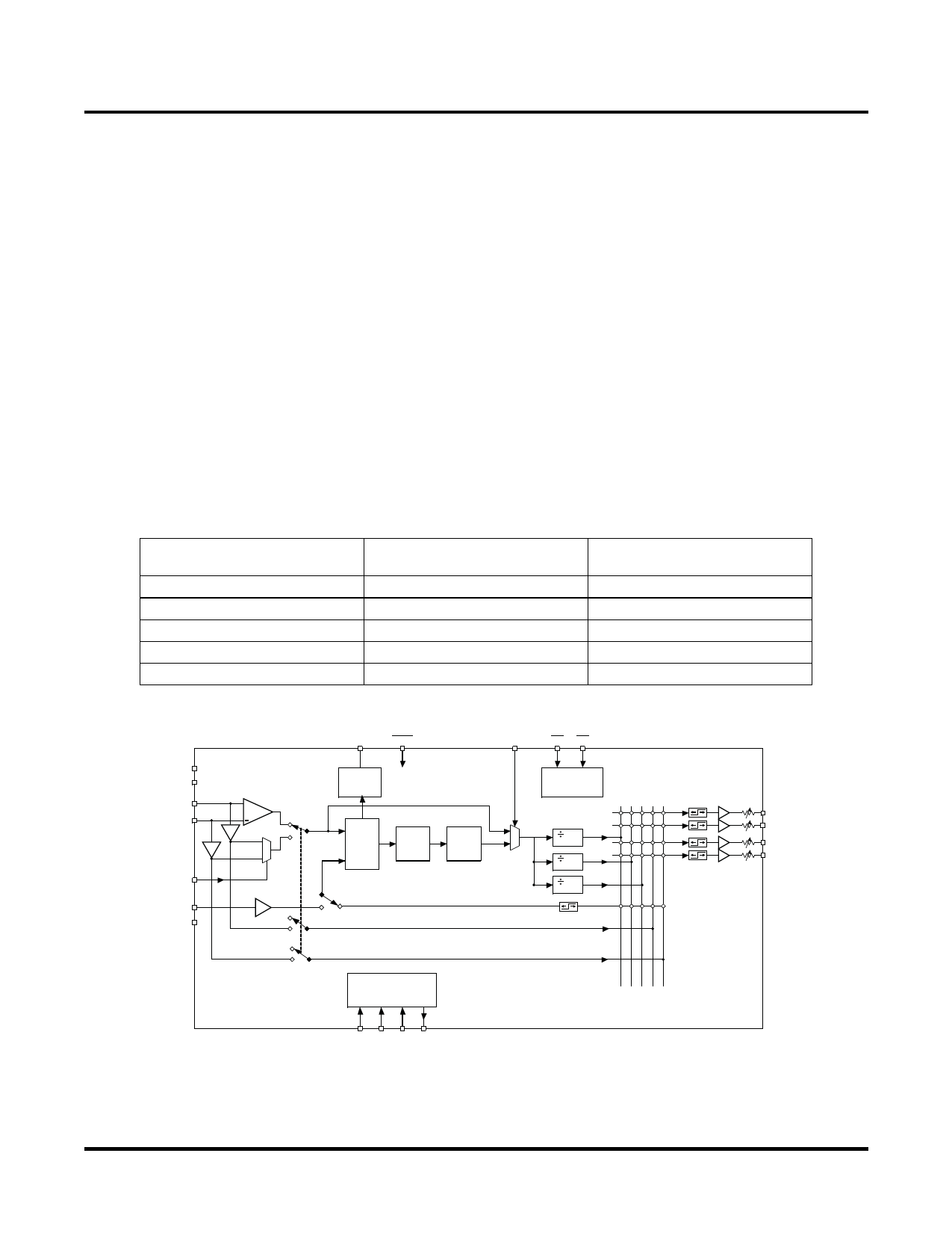
Figure 1. ispClock5304S Functional Block Diagram
LOCK
RESET
PLL_ BYPASS OEX OEY
VTT_REFA
VTT_REFB
REFA_REFP
REFB_REFN
REFSEL
FBK
VTT_FBK
+
0
1
LOCK
DETECT
PHASE
DETECT
LOOP
FILTER
VCO
OUTPUT ENABLE
CONTROLS
OUTPUT ROUTING
MATRIX
SKEW
OUTPUT
CONTROL DRIVERS
OUTPUT
DIVIDERS
1
V0
0
5-bit
BANK_0A
BANK_0B
BANK_1A
V1
BANK_1B
5-bit
SKEW
OUTPUT
V2
CONTROL DRIVERS
5-bit
JTAG INTERFACE
TDI TMS TCK TDO
2
Share Link: 