RMWB11001 데이터 시트보기 (PDF) - Fairchild Semiconductor
부품명
상세내역
제조사
RMWB11001 Datasheet PDF : 6 Pages
| |||
0.0 0.11
1.3
1.145
0.873
0.720
0.567
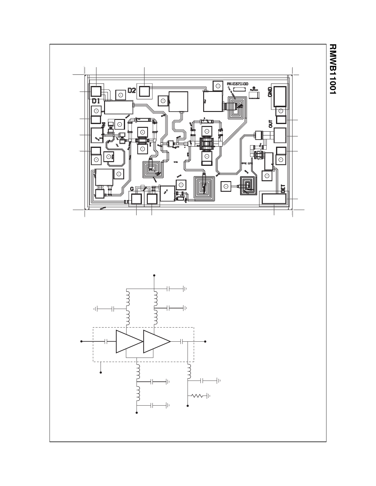
Figure 1. Chip Layout and Bond Pad Locations
0.577
2.0
1.3
0.873
0.720
0.567
0.106
0.0
0.0
0.5 0.65
0.0
1.828 2.0
Chip Size is 2.0mm x 1.3mm X 100µm. Back of chip is RF and DC Ground.
Figure 2. Recommended Application Schematic Circuit Diagram
L = Bond Wire
Inductance
Drain Supply
Vd=+4 V
10,000pF
100pF
L
L 100pF
L
L
RF IN
RF OUT
MMIC Chip
Ground
(Back of Chip)
L
L
100pF
L
100pF
3 kΩ
Gate
Supply
Vg
10,000pF Output Power
Detector Voltage
Vdet
Note : Detector delivers approx.
0.5V DC into 3kΩ load resistor
for >+18 dBm output power. If
output power level detection is
not desired, do not make
connection to detector bond
pad.
©2004 Fairchild Semiconductor Corporation
RMWB11001 Rev. C
Share Link: 