ADT7411ARQZ10 데이터 시트보기 (PDF) - Analog Devices
부품명
상세내역
제조사
ADT7411ARQZ10
Analog Devices
ADT7411ARQZ10 Datasheet PDF : 36 Pages
| |||
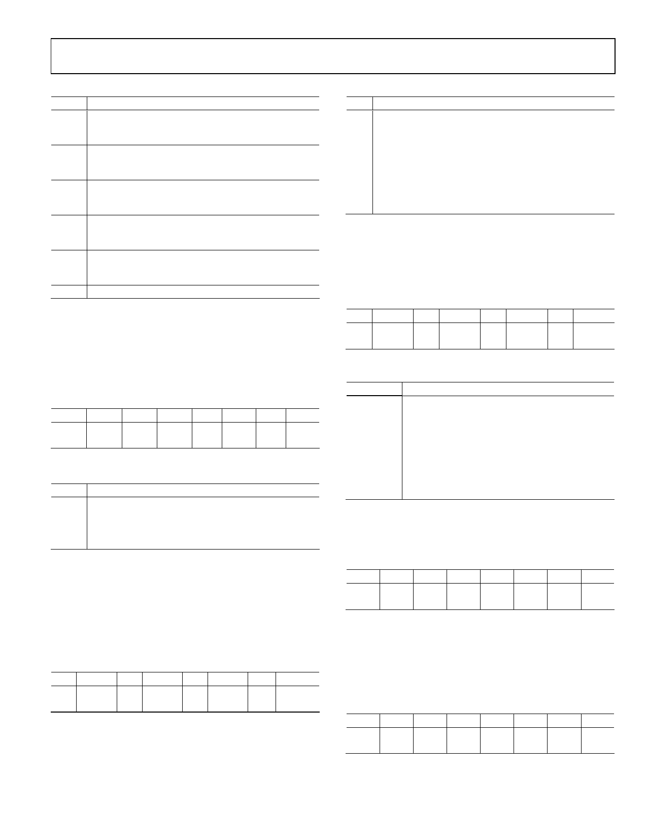
Table 11.
Bit Function
D0 1 when AIN5 voltage is greater than the corresponding
VHIGH limit. 1 when AIN5 voltage is less than or equal to
the corresponding VLOW limit.
D1 1 when AIN6 voltage is greater than the corresponding
VHIGH limit. 1 when AIN6 voltage is less than or equal to
the corresponding VLOW limit.
D2 1 when AIN7 voltage is greater than the corresponding
VHIGH limit. 1 when AIN7 voltage is less than or equal to
the corresponding VLOW limit.
D3 1 when AIN8 voltage is greater than the corresponding
VHIGH limit. 1 when AIN8 voltage is less than or equal to
the corresponding VLOW limit.
D4
1 when VDD value is greater than the corresponding
VHIGH limit. 1 when VDD is less than or equal to the
corresponding VLOW limit.
D5:D7 Reserved
Internal Temperature Value/VDD Value Register LSBs
(Read-Only) [Add. = 03h]
This internal temperature value and VDD value register is an
8-bit read-only register. It stores the 2 LSBs of the 10-bit temp-
erature reading from the internal temperature sensor and also
the 2 LSBs of the 10-bit supply voltage reading.
Table 12. Internal Temperature/VDD LSBs
D7 D6 D5 D4 D3 D2 D1 D0
N/A N/A N/A N/A V1 LSB T1 LSB
N/A N/A N/A N/A 0* 0*
0* 0*
*Default settings at power-up.
Table 13.
Bit Function
D0 LSB of Internal Temperature Value.
D1 B1 of Internal Temperature Value.
D2
LSB of VDD Value.
D3
B1 of VDD Value.
External Temperature Value and Analog Inputs1 to 4
Register LSBs (Read-Only) [Address = 04h]
This is an 8-bit read-only register. Bits D2–D7 store the 2 LSBs
of the analog inputs AIN2–AIN4. Bits D0 and D1 are used to
store the 2 LSBs of either the external temperature value or
AIN1 input value. The type of input for D0 and D1 is selected
by Bits 1:2 of the Control Configuration 1 register.
Table 14. External Temperature and AIN1–4 LSBs
D7 D6
D5 D4
D3 D2
D1
A4 A4LSB
A3 A3LSB
A2 A2LSB
T/A
0* 0*
0* 0*
0* 0*
0*
*Default settings at power-up.
D0
T/ALSB
0*
ADT7411
Table 15
Bit Function
D0 LSB of External Temperature Value or AIN1 Value.
D1 Bit 1 of External Temperature Value or AIN1 Value.
D2 LSB of AIN2 Value.
D3 Bit 1 of AIN2 Value.
D4 LSB of AIN3 Value.
D5 Bit 1 of AIN3 Value.
D6 LSB of AIN4 Value.
D7 Bit 1 of AIN4 Value.
Analog Inputs 5 to 8 Registers LSBs (Read-Only)
[Add. = 05h]
This is an 8-bit read-only register. Bits D0 to D7 store the 2 LSBs
of the analog inputs AIN5 to AIN8. The MSBs are stored in
Registers 0Ch to 0Fh.
Table 16. External Temperature and AIN5 to AIN8 LSBs
D7 D6
D5 D4
D3 D2
D1 D0
A8 A8LSB
A7 A7LSB
A6 A6LSB
A5 A5LSB
0* 0*
0* 0*
0* 0*
0* 0*
*Default settings at power-up.
Table 17.
Bit
D0
D1
D2
D3
D4
D5
D6
D7
Function
LSB of AIN5 Value.
Bit 1 of AIN5 Value.
LSB of AIN6 Value.
Bit 1 of AIN6 Value.
LSB of AIN7 Value.
Bit 1 of AIN7 Value.
LSB of AIN8 Value.
Bit 1 of AIN8 Value.
VDD Value Register MSBs (Read-Only) [Address = 06h]
This 8-bit read-only register stores the supply voltage value. The
8 MSBs of the 10-bit value are stored in this register.
Table 18. VDD Value MSBs
D7 D6 D5 D4 D3 D2 D1 D0
V9 V8 V7 V6 V5 V4 V3 V2
x*
x*
x*
x*
x*
x*
x*
x*
*Loaded with VDD value after power-up.
Internal Temperature Value Register MSBs (Read-Only)
[Address = 07h]
This 8-bit read-only register stores the internal temperature
value from the internal temperature sensor in twos complement
format. This register stores the 8 MSBs of the 10-bit value.
Table 19. Internal Temperature Value MSBs
D7 D6 D5 D4 D3 D2 D1 D0
T9 T8 T7 T6 T5 T4 T3 T2
0* 0* 0* 0* 0* 0* 0* 0*
*Default settings at power-up.
Rev. A | Page 21 of 36
Share Link: 