74LVC244ABQ(2009) 데이터 시트보기 (PDF) - NXP Semiconductors.
부품명
상세내역
제조사
74LVC244ABQ Datasheet PDF : 18 Pages
| |||
NXP Semiconductors
74LVC244A; 74LVCH244A
Octal buffer/line driver; 3-state
VI
nOE input
GND
VCC
output
LOW-to-OFF
OFF-to-LOW
VOL
VOH
output
HIGH-to-OFF
OFF-to-HIGH
GND
VM
tPLZ
tPZL
tPHZ
VX
VY
VM
tPZH
VM
outputs
enabled
outputs
disabled
outputs
enabled
mna362
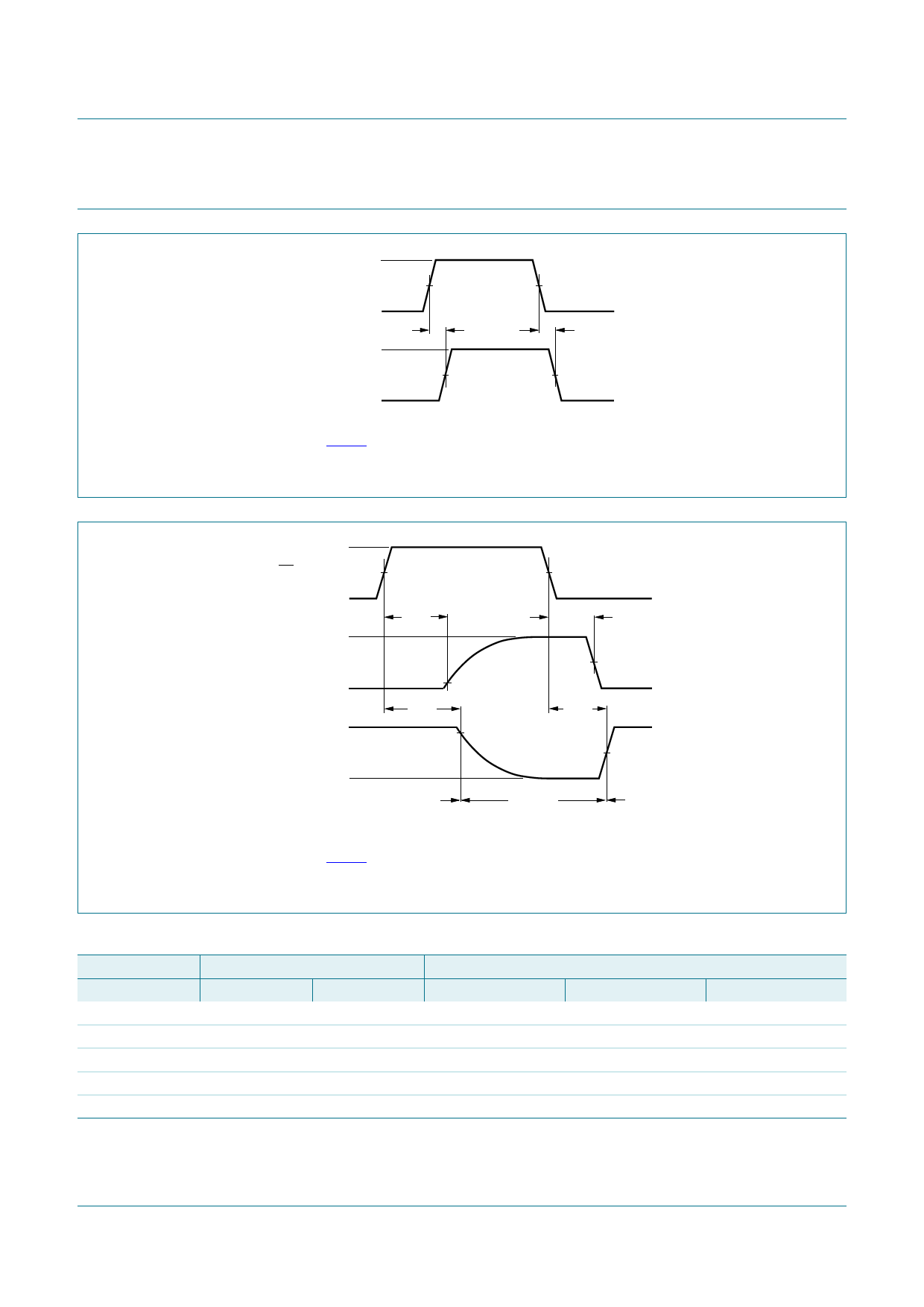
Fig 7.
Measurement points are given in Table 8.
Logic levels: VOL and VOH are typical output voltage levels that occur with the output load.
3-state enable and disable times.
Table 8. Measurement points
Supply voltage Input
VCC
1.2 V
2.7 V
VI
VCC
2.7 V
3.0 V to 3.6 V
2.7 V
VM
0.5 × VCC
1.5 V
1.5 V
Output
VM
0.5 × VCC
1.5 V
1.5 V
VX
VOL + 0.1 V
VOL + 0.3 V
VOL + 0.3 V
VY
VOH − 0.1 V
VOH − 0.3 V
VOH − 0.3 V
74LVC_LVCH244A_6
Product data sheet
Rev. 06 — 13 August 2009
© NXP B.V. 2009. All rights reserved.
9 of 18
Share Link: 