XRT91L32 데이터 시트보기 (PDF) - Exar Corporation
부품명
상세내역
제조사
XRT91L32 Datasheet PDF : 37 Pages
| |||
XRT91L32
STS-12/STM-4 OR STS-3/STM-1 SONET/SDH TRANSCEIVER
xr
REV. 1.0.2
NAME
PARAMETER
MIN
TYP
MAX UNITS
OCLKFREQ
Frequency output
620
624 MHz
OCYCDUTY Clock output duty cycle (’1010’ data pattern)
45
55
%
Jitter specification is defined using a 12kHz to 1.3/5MHz LP-HP single-pole filter.
1These reference clock jitter limits are required for the outputs to meet SONET system level jitter requirements (<10 mUIrms).
2Required to meet SONET output frequency stability requirements.
3.5 Loop Timing and Clock Control
Two types of loop timing are possible in the XRT91L32.
In the internal loop timing mode, loop timing is controlled by the LOOPTIME pin. This mode is selected by
asserting the LOOPTIME signal to a high level. When the loop timing mode is activated, the CMU synthesized
hi-speed reference clock input to the Retimer is replaced with the hi-speed internally recovered receive clock
coming from the CDR. Under this condition both the transmit and receive sections are synchronized to the
internally recovered receive clock. Loop time mode directly locks the Retimer to the recovered receive clock.
In external loop timing mode, the XRT91L32 allows the user the flexibility of using an externally recovered
receive clock for retiming the high speed serial data. First, the CDRDIS input pin should be set high. By doing
so, the internal CDR is disabled and bypassed and the XRT91L32 will sample the incoming high speed serial
data on RXIP/N with the externally recovered receive clock connected to the XRXCLKIP/N inputs. In this state,
the receive clock de-jittering and recovery is done externally and fed thru XRXCLKIP/N and the XRT91L32 will
sample RXIP/N on the rising edge of XRXCLKIP/N. Secondly, the LOOPTIME pin must also be set high in
order to select the externally recovered receive clock on XRXCLKIP/N as the reference clock source for the
transmit serial data output stream TXOP/N.
Table 13 provides configuration for selecting the loop timing and clock recovery modes. The use of the on-chip
CDR or an external recovered clock in loop timing applications is shown in Figure 14.
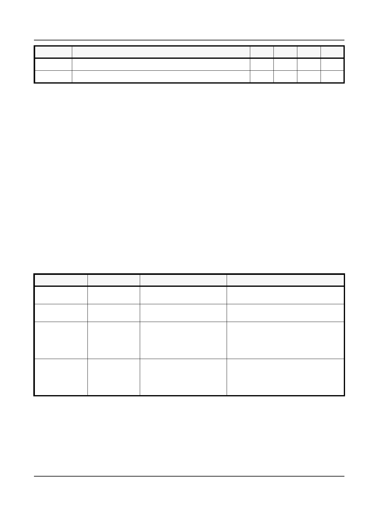
TABLE 13: LOOP TIMING AND CLOCK RECOVERY CONFIGURATIONS
CDRDIS
LOOPTIME
TRANSMIT CLOCK SOURCE
RECEIVE CLOCK SOURCE
0
0
Clock Multiplier Unit
CDR Enabled.
Clock and Data recovery by internal CDR
0
1
Internal CDR
CDR Enabled.
Clock and Data recovery by internal CDR
CDR Disabled.
Externally recovered Receive Clock from
1
0
Clock Multiplier Unit
XRXCLKIP/N
622.08/155.52 Mbps data on RXIP/N sampled at
rising edge of XRXCLKIP/N
CDR Disabled.
Externally recovered Receive Clock from
1
1
External CDR thru XRXCLKIP/N
XRXCLKIP/N
622.08/155.52 Mbps data on RXIP/N sampled at
rising edge of XRXCLKIP/N
24
Share Link: 