051AC 데이터 시트보기 (PDF) - STMicroelectronics
부품명
상세내역
제조사
051AC Datasheet PDF : 67 Pages
| |||
TL05x, TL05xA
ENHANCED-JFET LOW-OFFSET
OPERATIONAL AMPLIFIERS
SLOS178A – FEBRUARY 1997 - REVISED FEBRUARY 2003
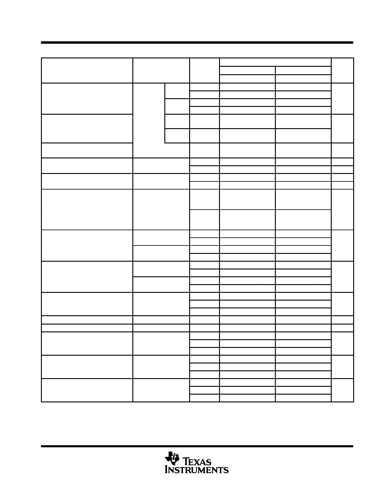
TL051I and TL051AI electrical characteristics at specified free-air temperature
TL051I, TL051AI
VIO
aVIO
PARAMETER
Input offset voltage
Temperature coefficient of
input offset voltage‡
TEST CONDITIONS
TA†
VO = 0,
VIC = 0,
RS = 50 Ω
TL051I
TL051AI
TL051I
TL051AI
25°C
Full range
25°C
Full range
25°C to
85°C
25°C to
85°C
VCC± = ±5 V
MIN TYP MAX
0.75 3.5
5.3
0.55 2.8
4.6
7
8
VCC± = ±15 V
MIN TYP MAX
0.59 1.5
3.3
0.35 0.8
2.6
UNIT
mV
8
µV/°C
8
25
Input offset-voltage
long-term drift§
25°C
0.04
0.04
µV/mo
IIO
Input offset current
IIB
Input bias current
VO = 0,
VIC = 0,
See Figure 5
VO = 0,
VIC = 0,
See Figure 5
25°C
85°C
25°C
85°C
4 100
0.06
10
20 200
0.6
20
5 100 pA
0.07
10 nA
30 200 pA
0.7
20 nA
VICR
Common-mode input
voltage range
–1 –2.3
–11 –12.3
25°C
to
to
to
to
4 5.6
11 15.6
V
–1
–11
Full range
to
to
4
11
Maximum positive peak
VOM + output voltage swing
RL = 10 kΩ
RL = 2 kΩ
25°C
3 4.2
13 13.9
Full range
3
13
V
25°C
2.5 3.8
11.5 12.7
Full range
2.5
11.5
Maximum negative peak
VOM – output voltage swing
RL = 10 kΩ
RL = 2 kΩ
25°C
–2.5 –3.5
–12 –13.2
Full range –2.5
–12
V
25°C
–2.3 –3.2
–11 –12
Full range –2.3
–11
AVD
Large-signal differential
voltage amplification¶
RL = 2 kΩ
25°C
–40°C
85°C
25
59
30
74
20
43
50 105
60 145
30
76
V/mV
ri
Input resistance
25°C
1012
1012
Ω
ci
Input capacitance
CMRR
Common-mode
rejection ratio
VIC = VICRmin,
VO = 0,
RS = 50 Ω
25°C
25°C
–40°C
85°C
10
65
85
65
83
65
84
12
pF
75
93
75
90
dB
75
93
kSVR
Supply-voltage rejection
ratio (∆VCC±/∆VIO)
VO = 0,
RS = 50 Ω
25°C
–40°C
85°C
75
99
75
98
75
99
75
99
75
98
dB
75
99
25°C
2.6 3.2
2.7 3.2
ICC
Supply current
VO = 0,
No load
–40°C
85°C
2.4 3.2
2.5 3.2
2.6 3.2 mA
2.6 3.2
† Full range is –40°C to 85°C
‡ This parameter is tested on a sample basis for the TL051A. For other test requirements, please contact the factory. This statement has no bearing
on testing or nontesting of other parameters.
§ Typical values are based on the input offset-voltage shift observed through 168 hours of operating life test at TA = 150°C, extrapolated to
TA = 25°C using the Arrhenius equation, and assuming an activation energy of 0.96 eV.
¶ For VCC± = ±5 V, VO = ±2.3 V, or for VCC± = ±15 V, VO = ±10 V.
• POST OFFICE BOX 655303 DALLAS, TEXAS 75265
7
Share Link: 