TK65025 데이터 시트보기 (PDF) - Toko America Inc
부품명
상세내역
제조사
TK65025 Datasheet PDF : 12 Pages
| |||
TK65025
standpoint for the TK65025, this is essentially guaran-
teed when using a single battery cell to power the
converter.
Now, plugging in worst case conditions, the inductor
value can be determined by simply transforming the
above equation in terms of “L”:
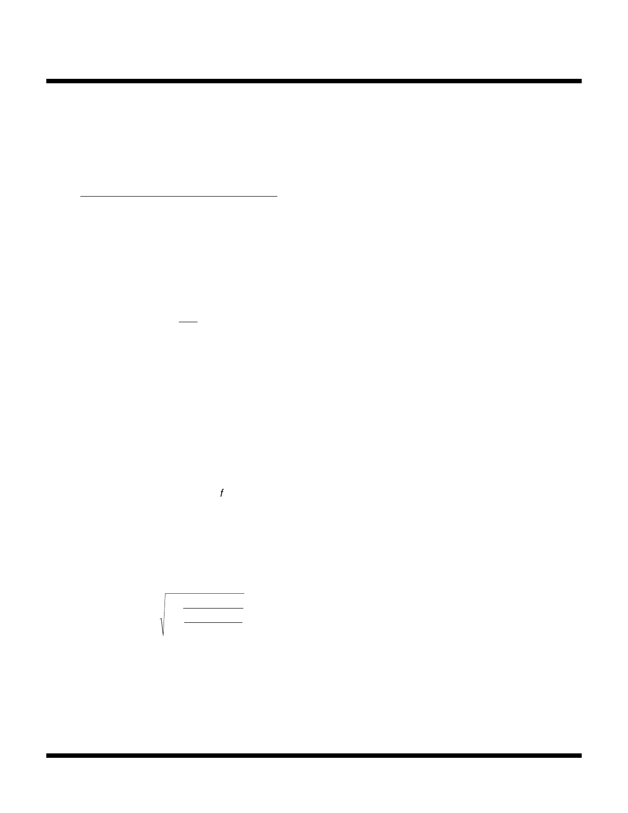
[ ] LMIN
=
V2
I(MIN)
D(MIN)
2 f I (MAX) O(MAX) VO(MIN) + VF(MAX)
−
V I( MIN )
2
(3)
where “VF(MAX)” is best approximated by the diode forward
voltage at about two-thirds of the peak diode current
value. The peak diode current is the same as the peak
input current, the peak switch current, and the peak
inductor current. The formula is:
I PK = VID
(4)
fL
Some reiteration is implied because “L” is a function
of “VF” which is a function of “IPK” which, in turn, is a function
of “L”. The best way into this loop is to first approximate
“VF”, determine “L”, determine “IPK”, and then determine a
new “VF”. Then, if necessary, reiterate.
When selecting the actual inductor, it is necessary to
make sure that the peak current rating of the inductor (i.e.,
the current which causes the core to saturate) is greater
than the maximum peak current that the inductor will
encounter. To determine the maximum peak current, use
Eq. (4) again, but this time plugging in maximum values for
“VI” and “D”, and minimum values for “f ” and “L”.
It may also be necessary when selecting the inductor to
check the rms current rating of the inductor. Whereas
peak current rating is determined by core saturation, rms
current rating is determined by wire size and power
dissipation in the wire resistance. The inductor rms
current is given by:
I L(RMS) = I PK
D+
VO
I PK f L
+ VF − VI
(5)
3
where “IPK” is the same maximized value that was just
used to check against inductor peak current rating, and
the term in the numerator within the radical that is added
to the [on-time] duty ratio, “D”, is the off-time duty ratio.
Toko America, Inc. offers a wide range of inductor
values and sizes to accommodate varying power level
requirements. The following series of Toko inductors
Page 6
work especially well with the TK65025: 10RF, 12RF, 3DF,
D73, and D75. The 5CA series can be used for
isolated-output applications, although such design objec-
tives are not considered here.
Other Converter Components
In choosing a diode, parameters worthy of consider-
ation are: forward voltage, reverse leakage, and capaci-
tance. The biggest efficiency loss in the converter is due
to the diode forward voltage. A schottky diode is typically
chosen to minimize this loss. Possible choices for Schottky
diodes are: LL103A from ITT MELF case; 1N5017 from
Motorola (through hole case); MBR0530 from Motorola
(surface mount) or 15QS02L from Nihon EC (surface
mount).
Reverse leakage current is generally higher in schottkys
than in pin-junction diodes. If the converter spends a good
deal of the battery lifetime operating at very light load (i.e.,
the system under power is frequently in a standby mode),
then the reverse leakage current could become a substan-
tial fraction of the entire average load current, thus degrad-
ing battery life. So don’t dramatically oversize the schottky
diode if this is the case.
Diode capacitance isn’t likely to make much of an
undesirable contribution to switching loss at this relatively
low switching frequency. It can, however, increase the
snubber dissipation requirement.
The snubber (optional) is composed of a series RC
network from the switch pin to ground (or to the output or
input if preferred). Its function is to dampen the resonant
LC circuit which rings during the inductor current deadtime.
When the current flowing in the inductor through the output
diode decays to zero, the parasitic capacitance at the
switch pin from the switch, the diode, and the inductor
winding has energy which rings back into the inductor,
flowing back into the battery. If there is no snubbing, it is
feasible that the switch pin voltage could ring below
ground. Although the IC is well protected against latchup,
this ringing may be undesirable due to radiated noise. In
order to do an effective job, the snubber capacitor should
be large (e.g., 5~20 times) in comparison to the parasitic
capacitance. If it is unnecessarily large, then it dissipates
extra energy every time the converter switches. The
resistor of the snubber should be chosen such that it drops
a substantial voltage as the ringing parasitic capacitance
attempts to pull the snubber capacitor along for the ride. If
the resistor is too small (e.g., zero), then the snubber
capacitance just adds to the ringing energy. If the resistor
is too large (e.g., infinite) then it effectively disengages the
snubber capacitor from fighting the ringing.
The output capacitor, the capacitor connected from the
February, 1997 Toko, Inc.
Share Link: 