SI4702-C19 데이터 시트보기 (PDF) - Silicon Laboratories
부품명
상세내역
제조사
SI4702-C19 Datasheet PDF : 46 Pages
| |||
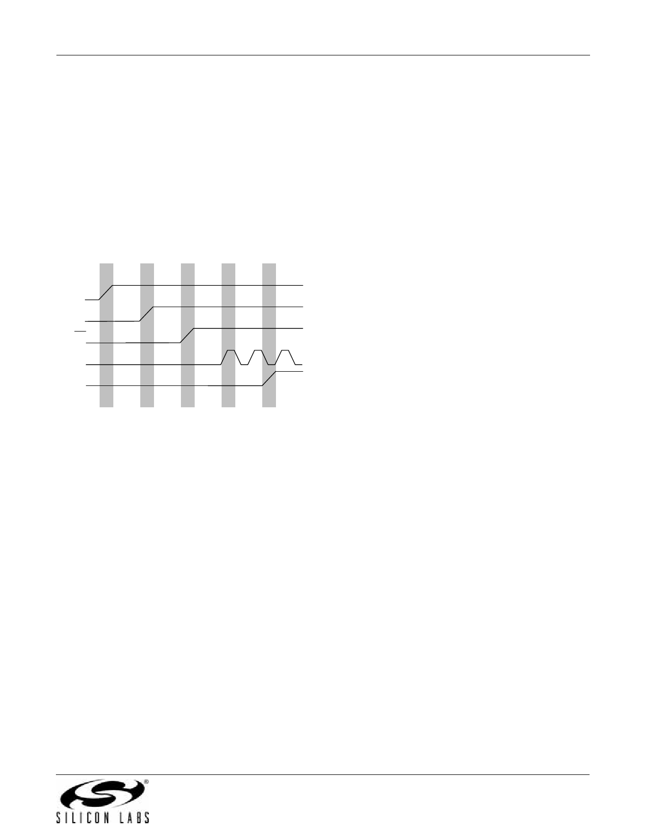
To power up the device (after power down):
1. Note that VIO is still supplied in this scenario. If VIO is not
supplied, refer to device initialization procedure above.
2. (Optional) Set the AHIZEN bit low to disable the dc bias of
0.5 x VIO volts at the LOUT and ROUT pins, but preserve
the states of the other bits in Register 07h. Note that in
powerup the LOUT and ROUT pins are set to the common
mode voltage specified in Table 8 on page 12, regardless
of the state of AHIZEN.
3. Supply VA and VD.
4. Provide RCLK. Refer to AN230 when using internal
oscillator.
5. Set the ENABLE bit high and the DISABLE bit low to
powerup the device.
VA,VD Supply
VIO Supply
RST Pin
RCLK Pin
ENABLE Bit
1
2
3
4
5
Figure 9. Initialization Sequence
4.12. Programming Guide
Refer to "AN230: Si4700/01 Programming Guide" for
control interface programming information.
Si4702/03-C19
Rev. 1.1
21
Share Link: 