MAX155BEPI(2012) 데이터 시트보기 (PDF) - Maxim Integrated
부품명
상세내역
제조사
MAX155BEPI Datasheet PDF : 20 Pages
| |||
MAX155/MAX156
8-/4-Channel ADCs with Simultaneous
T/Hs and Reference
Detailed Description
ADC Operation
The MAX155/MAX156 contain a 3.6µs successive approx-
imation ADC and 8/4 track-and-hold (T/H) inputs. When a
conversion is started, all AIN inputs are simultaneously
sampled. All channels sample whether or not they are
selected for the conversion. Either a single-channel or
multichannel conversion may be requested and channel
configurations may be mixed, ADC results are then stored
in an internal RAM.
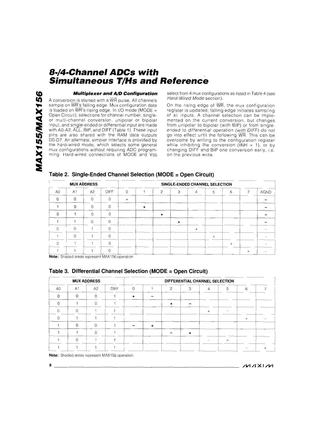
In hard-wired mode (see the Multiplexer and AID
Configurations section) multichannel conversions are
initiated with one write operation. In input/output (I/O)
mode, multichannel configurations are set up prior to the
conversion by loading channel selections into the con-
figuration register. This register also selects single-ended/
differential, unipolar/bipolar (Figure 9), power-down, and
other functions. Each channel selection requires a sepa-
rate write operation (i.e. 8 writes for 8 channels), but only
after power-up. Once the desired channel arrangement
is loaded, each subsequent write converts all selected
channels without reconfiguring the multiplexer (mux). I/O
mode requires more write operations, but provides more
flexibility than hard-wired mode.
To access conversion results, successive RD pulses auto-
matically sence through RAM, beginning with channel 0.
Each RD pulse increments the RAM address counter,
which resets to 0 when WR goes low in multichannel
conversions. An arbitrary RAM location may also be read
by writing a 1 to INH while loading the RAM address (A0–
A2), and then performing a read operation.
Table 1. Multiplexer Configurations
PIN
NAME
FUNCTION
D0/A0
D1/A1
D2/A2
1 or 0
A0–A2 select a multiple channel for the configurations described below, or select a RAM address
for reading with a subsequent RD.
D3/PD
0
Normal ADC operation
1
Power-down reduces the power-supply current. Configuration data may be loaded and is
maintained during power-down.
D4/INH
0
A conversion starts when WR goes high
1
Inhibits the conversion when WR goes high. Allows mux configuration to be loaded and RAM
locations to be accessed without starting a conversion.
D5/BIP**
D6/DIFF**
0
Unipolar conversion (Figure 9a) for the channel specified by A0–A2. Input range = 0V to VREF.
1
Bipolar conversion (Figure 9b) for the channel specified by A0–A2. Input range = ±VREF.
0
Single-ended configuration for the channel specified by A0–A2 as described in Table 2
1
Differential contiguration for the channel specified by A0–A2 as described in Table 2
D7/ALL
0
All previously configured channels are converted. Data is read with consecutive RD pulses,
beginning with the lowest configured channel.
1
Only the channel specified by A2–A0 is converted. A single RD pulse reads the result of that
conversion.
•Configuration inputs are shared with data outputs D0-D7. The functions of D0-D7 are not described in this table.
••DIFF and BIP are not implemented on the current conversion, but go into effect on the.following conversion.
www.maximintegrated.com
Maxim Integrated │ 8
Share Link: 