MAX155BEPI(2012) 데이터 시트보기 (PDF) - Maxim Integrated
부품명
상세내역
제조사
MAX155BEPI Datasheet PDF : 20 Pages
| |||
MAX155/MAX156
8-/4-Channel ADCs with Simultaneous
T/Hs and Reference
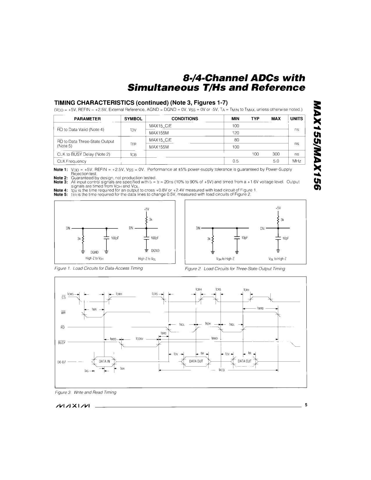
TIMING CHARACTERISTICS (Note 3, Figures 1-7) (continued)
(VDD = +5V, VREFIN = +2.5V. External Reference, VAGND = VDGND = 0V, VSS = 0V or -5V, TA = TMIN to TMAX, unless otherwise noted.)
PARAMETER
BUSY High to WR Delay (to update
configuration register) (Notes 2, 3)
SYMBOL
tBWD
CONDITIONS
MIN
TYP MAX UNITS
50
ns
CLK to WR Delay (Acquisition Time)
(Note 2)
BUSY High to RD Delay (Notes 2, 3)
Address-Setup Time
Address-Hold Time
RD to Data Valid (Note 4)
RD to Data Three-State Output (Note 5)
CLK to BUSY Delay (Note 2)
CLK Frequency
tACQ
tBRD
tAS
tAH
tDV
tTR
tCB
MAX15_C/E
MAX15_C/E
800
ns
50
ns
120
ns
0
ns
100
ns
80
ns
100
300
ns
0.5
5.0
MHz
Note 1: VDD = +5V, VREFIN = +2.5V, VSS = 0V. Performance at ±5% power-supply tolerance is guaranteed by Power-Supply
Rejection test.
Note 2: Guaranteed by design, not production tested.
Note 3: All input control signals are specified with tr = tf = 20ns (10% to 90% of +5V) and timed from a +1.6V voltage level. Output
signals are timed from VOH and VOL.
Note 4: tDV is the time required for an output to cross +0.8V or +2.4V measured with load circuit of Figure 1.
Note 5: tTR is the time required for the data lines to change 0.5V, measured with load circuits of Figure 2.
+5V
3kΩ
DN
3kΩ
100pF
DGND
HIGH-Z TO VOH
DN
100pF
DGND
HIGH-Z TO VOL
Figure 1. Load Circuits for Data-Access Timing
DN
10pF
3kΩ
VOH TO HIGH-Z
+5V
3kΩ
DN
10pF
VOL TO HIGH-Z
Figure 2. Load Circuits for Three-State Output Timing
www.maximintegrated.com
Maxim Integrated │ 5
Share Link: 