TB62715F 데이터 시트보기 (PDF) - Marktech Optoelectronics
부품명
상세내역
제조사
TB62715F
Marktech Optoelectronics
TB62715F Datasheet PDF : 10 Pages
| |||
TOSHIBA Bi-CMOS
Constant Current Interface Driver
TB62715F/FN
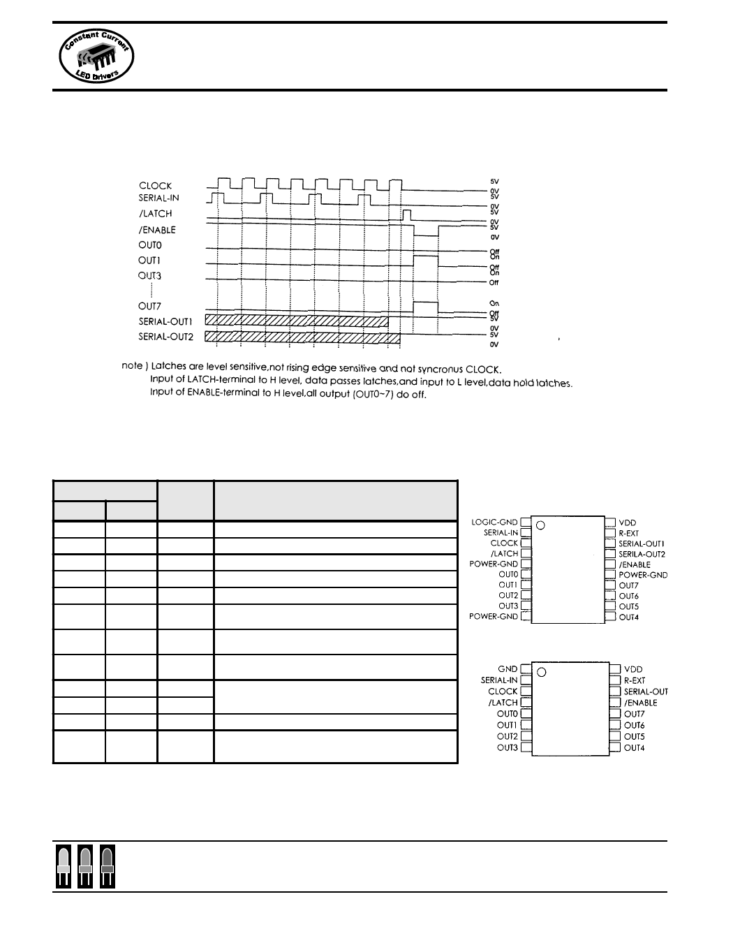
Timing Diagram:
Terminal Description & Pin Out:
PIN No.
SSOP20
5
6, 15
1
2
3
SSOP16
1
2
3
4
4
7~10,
11~14
5~12
16
13
18
14
17
19
15
PIN NAME
FUNCTION
HIGH/LOW Use Current Select.
POWER-GND GND terminal for control output
LOGIC-GND GND terminal for control logic
SERIAL-IN Input terminal of a serial-data for shift-register
CLOCK
Input terminal of a clock for data shift to up-edge.
/LATCH
Input terminal of a data strobe. Latches passes data with "H" level input
of LATCH-terminal, and hold data with "L" level input.
OUT0~7 Output terminals.
/ENABLE
Input terminal of output enable. All outputs (OUT0~7) do off with "H" level
input of ENABLE-terminal, and do on with "L" level input.
SERIAL-OUT1
Output terminal of a serial-data for next SERIAL-IN terminal.
SERIAL-OUT2
R-EXT
Input terminal of connects with a resister for to set up all output current.
20
16
VDD
5V Supply voltage terminal
marktech
optoelectronics
120 Broadway Menands, New York 12204
Toll Free: (888) 4LED-ICS Fax: (518) 432-7454
All specifications subject to change.
2
Share Link: 