MM74HC4538M 데이터 시트보기 (PDF) - Fairchild Semiconductor
부품명
상세내역
제조사
MM74HC4538M Datasheet PDF : 10 Pages
| |||
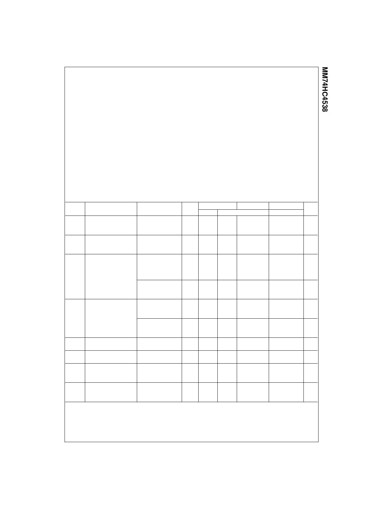
Absolute Maximum Ratings(Note 1)
(Note 2)
Recommended Operating
Conditions
Supply Voltage (VCC)
DC Input Voltage (VIN)
DC Output Voltage (VOUT)
Clamp Diode Current (IIK, IOK)
DC Output Current, per pin (IOUT)
DC VCC or GND Current, per pin (ICC)
Storage Temperature Range (TSTG)
Power Dissipation (PD)
(Note 3)
S.O. Package only
Lead Temperature (TL)
(Soldering 10 seconds)
−0.5 to +7.0V
−1.5 to VCC +1.5V
−0.5 to VCC +0.5V
±20 mA
±25 mA
±50 mA
−65°C to +150°C
600 mW
500 mW
260°C
Min Max Units
Supply Voltage (VCC)
2
6
V
DC Input or Output Voltage
0
VCC
V
(VIN, VOUT)
Operating Temperature Range (TA) −40 +85
°C
Input Rise or Fall Times
(Reset only)
(tr, tf) VCC = 2.0V
1000 ns
VCC = 4.5V
500
ns
VCC = 6.0V
400
ns
Note 1: Maximum Ratings are those values beyond which damage to the
device may occur.
Note 2: Unless otherwise specified all voltages are referenced to ground.
Note 3: Power Dissipation Temperature Derating: Plastic “N” Package: −
12mW/°C from 65°C to 85°C.
DC Electrical Characteristics (Note 4)
Symbol
Parameter
Conditions
VCC
TA = 25°C
TA = −40 to 85°C TA = −55 to 125°C
Units
Typ
Guaranteed Limits
VIH
Minimum HIGH Level Input
Voltage
2.0V
4.5V
1.5
1.5
3.15
3.15
1.5
V
3.15
V
6.0V
4.2
4.2
4.2
V
VIL
Maximum LOW Level Input
Voltage
2.0V
4.5V
0.5
0.5
1.35
1.35
0.5
V
1.35
V
6.0V
1.8
1.8
1.8
V
VOH
Minimum HIGH Level Output VIN = VIH or VIL
Voltage
|IOUT| ≤ 20 µA
2.0V
2.0
1.9
1.9
4.5V
4.5
4.4
4.4
1.9
V
4.4
V
6.0V
6.0
5.9
5.9
5.9
V
VIN = VIH or VIL
|IOUT| ≤ 4.0 mA
|IOUT| ≤ 5.2 mA
VOL
Maximum LOW Level Output VIN = VIH or VIL
Voltage
|IOUT| ≤ 20 µA
4.5V
3.98
3.84
6.0V
5.48
5.34
2.0V
0
0.1
0.1
4.5V
0
0.1
0.1
6.0V
0
0.1
0.1
3.7
V
5.2
V
0.1
V
0.1
V
0.1
V
VIN = VIH or VIL
|IOUT| ≤ 4.0 mA
|IOUT| ≤ 5.2 mA
IIN
Maximum Input Current
VIN = VCC or GND
(Pins 2, 14) (Note 5)
4.5V
6.0V
6.0V
0.26
0.33
0.26
0.33
±0.1
±1.0
0.4
V
0.4
V
±1.0
µA
IIN
Maximum Input Current
VIN = VCC or GND
(all other pins)
6.0V
±0.1
±1.0
±1.0
µA
ICC
Active
Maximum Active Supply
Current
Pins 2, 14 = 0.5 VCC
Q1, Q2 = HIGH
6.0V
150
250
400
µA
ICC
Maximum Quiescent Supply
Quiescent Current
VIN = VCC or GND
Pins 2, 14 = OPEN
Q1, Q2 = LOW
6.0V
130
220
350
µA
VIN = VCC or GND
Note 4: For a power supply of 5V ±10% the worst case output voltages (VOH, and VOL) occur for HC at 4.5V. Thus the 4.5V values should be used when
designing with this supply. Worst case VIH and VIL occur at VCC = 5.5V and 4.5V respectively. (The VIH value at 5.5V is 3.85V.) The worst case leakage cur-
rent (IIN, ICC, and IOZ) occur for CMOS at the higher voltage and so the 6.0V values should be used.
5
www.fairchildsemi.com
Share Link: 