MC74VHC1G32 데이터 시트보기 (PDF) - ON Semiconductor
부품명
상세내역
제조사
MC74VHC1G32 Datasheet PDF : 14 Pages
| |||
MC74VHC1G32,
MC74VHC1GT32
Single 2-Input OR Gate
The MC74VHC1G32 / MC74VHC1GT32 is a single 2−input OR
Gate in tiny footprint packages. The MC74VHC1G32 has
CMOS−level input thresholds while the MC74VHC1GT32 has
TTL−level thresholds.
The input structures provide protection when voltages up to 5.5 V
are applied, regardless of the supply voltage. This allows the device to
be used to interface 5 V circuits to 3 V circuits. The output structures
also provide protection when VCC = 0 V and when the output voltage
exceeds VCC. These input and output structures help prevent device
destruction caused by supply voltage − input/output voltage mismatch,
battery backup, hot insertion, etc.
Features
• Designed for 2.0 V to 5.5 V VCC Operation
• 3.5 ns tPD at 5 V (typ)
• Inputs/Outputs Over−Voltage Tolerant up to 5.5 V
• IOFF Supports Partial Power Down Protection
• Source/Sink 8 mA at 3.0 V
• Available in SC−88A, SC−74A, TSOP−5, SOT−553, SOT−953 and
UDFN6 Packages
• Chip Complexity < 100 FETs
• NLV Prefix for Automotive and Other Applications Requiring
Unique Site and Control Change Requirements; AEC−Q100
Qualified and PPAP Capable
• These Devices are Pb−Free, Halogen Free/BFR Free and are RoHS
Compliant
IN A
≥1
OUT Y
IN B
Figure 1. Logic Symbol
5
1
1
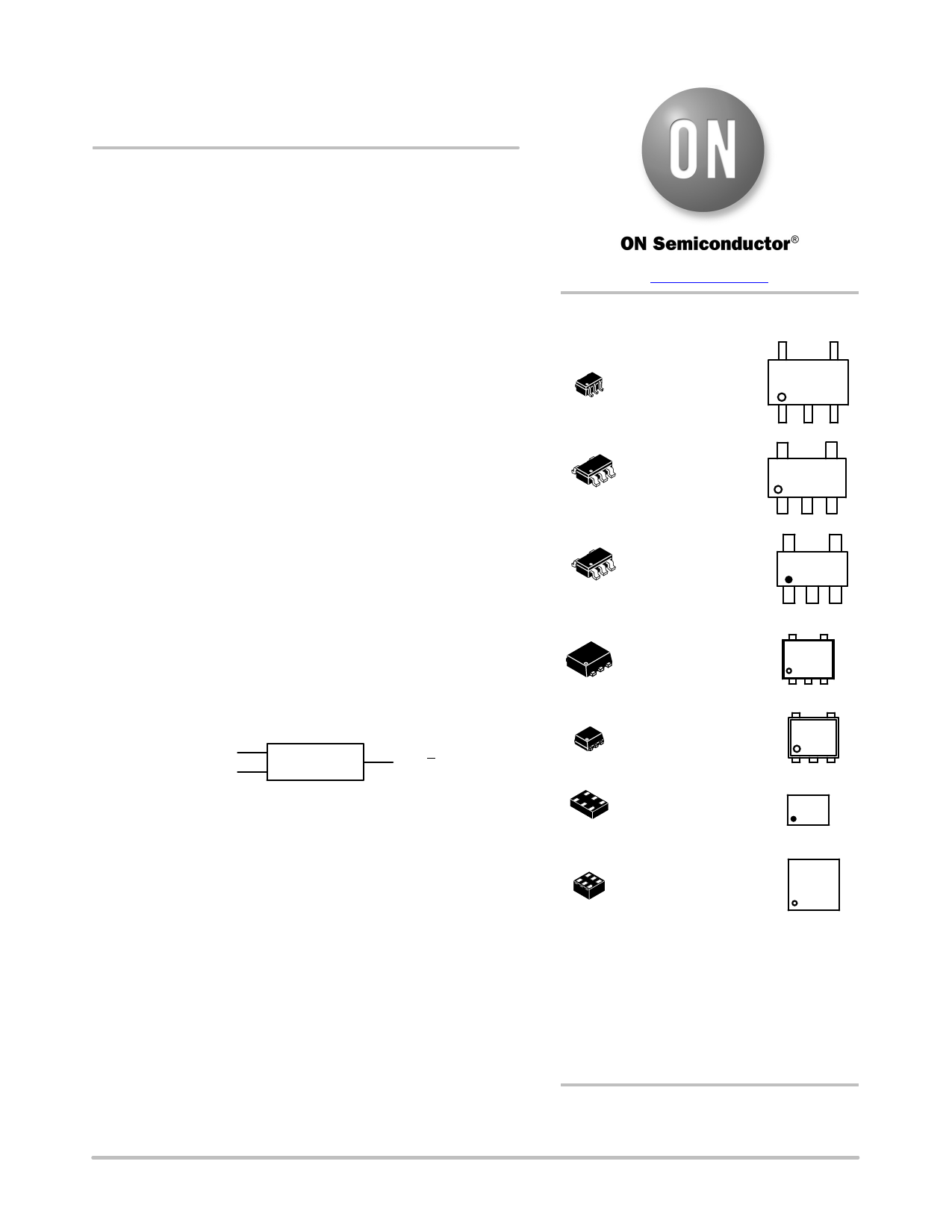
www.onsemi.com
MARKING
DIAGRAMS
SC−88A
DF SUFFIX
CASE 419A
XX MG
G
SC−74A
DBV SUFFIX
CASE 318BQ
XXX MG
G
TSOP−5
DT SUFFIX
CASE 483
SOT−553
XV5 SUFFIX
CASE 463B
5
XX MG
G
1
XX MG
G
SOT−953
P5 SUFFIX
CASE 527AE
UDFN6
1.45 x 1.0
CASE 517AQ
XM
1
XM
UDFN6
1.0 x 1.0
CASE 517BX
XM
1
XX
= Specific Device Code
M
= Date Code*
G
= Pb−Free Package
(Note: Microdot may be in either location)
*Date Code orientation and/or position may
vary depending upon manufacturing location.
© Semiconductor Components Industries, LLC, 2011
November, 2018 − Rev. 21
ORDERING INFORMATION
See detailed ordering, marking and shipping information in the
package dimensions section on page 7 of this data sheet.
1
Publication Order Number:
MC74VHC1G32/D
Share Link: 