MC74ACT374DWR2G(2015) 데이터 시트보기 (PDF) - ON Semiconductor
부품명
상세내역
제조사
MC74ACT374DWR2G Datasheet PDF : 10 Pages
| |||
TRUTH TABLE
Inputs
Dn
CP
H
L
X
X
H = HIGH Voltage Level
L = LOW Voltage Level
X = Immaterial
Z = High Impedance
= LOW-to-HIGH Transition
MC74AC374, MC74ACT374
Outputs
OE
On
L
H
L
L
H
Z
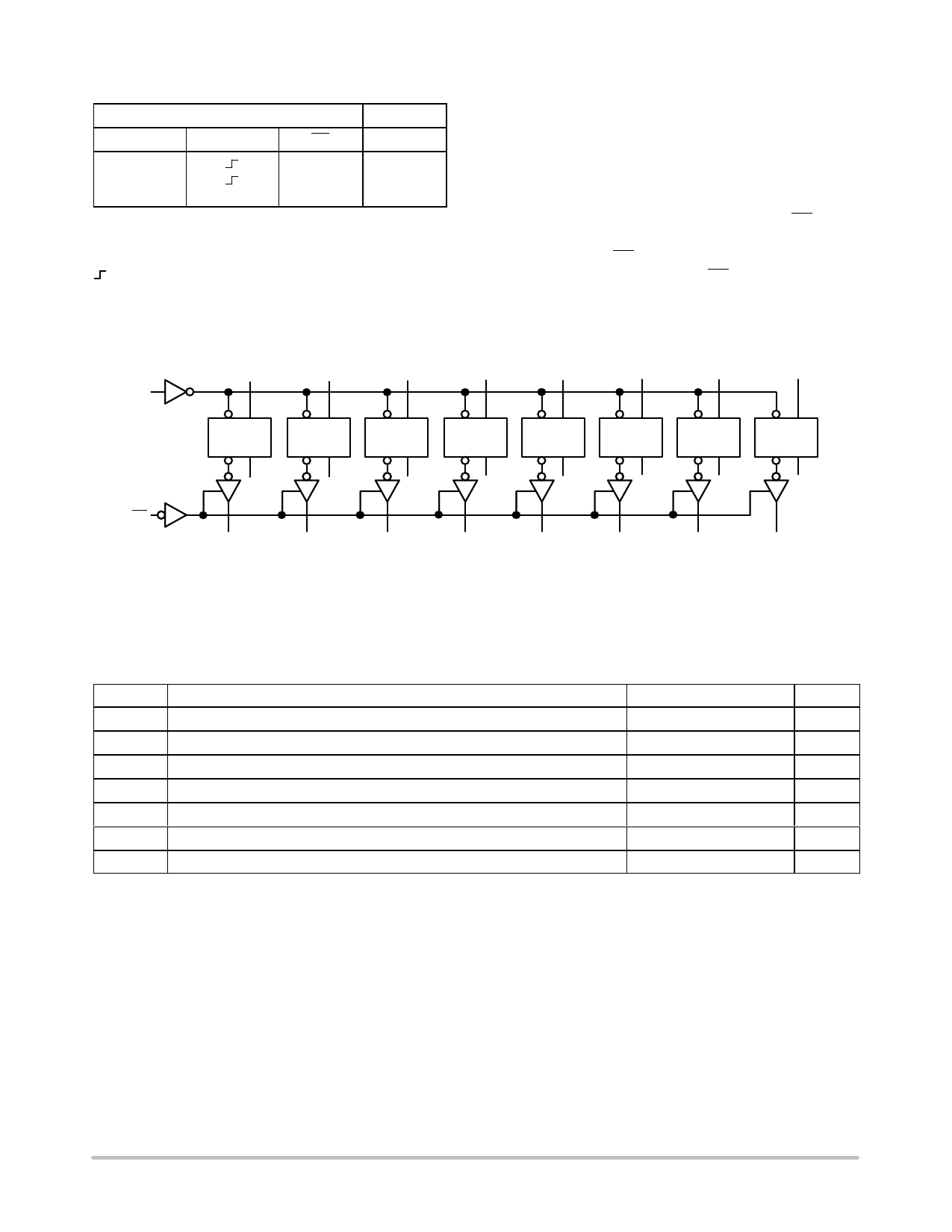
FUNCTIONAL DESCRIPTION
The MC74AC374/74ACT374 consists of eight edge−
triggered flip−flops with individual D−type inputs and
3−state true outputs. The buffered clock and buffered Output
Enable are common to all flip−flops. The eight flip−flops
will store the state of their individual D inputs that meet the
setup and hold time requirements on the LOW−to−HIGH
Clock (CP) transition. With the Output Enable (OE) LOW,
the contents of the eight flip−flops are available at the
outputs. When the OE is HIGH, the outputs go to the high
impedance state. Operation of the OE input does not affect
the state of the flip−flops.
D0
D1
D2
D3
D4
D5
D6
D7
CP
CP D
QQ
CP D
QQ
CP D
QQ
CP D
QQ
CP D
QQ
CP D
QQ
CP D
QQ
CP D
QQ
OE
O0
O1
O2
O3
O4
O5
O6
O7
NOTE: That this diagram is provided only for the understanding of logic
operations and should not be used to estimate propagation delays.
Figure 3. Logic Diagram
www.onsemi.com
2
Share Link: 