MC06XSD200FK 데이터 시트보기 (PDF) - Freescale Semiconductor
부품명
상세내역
제조사
MC06XSD200FK Datasheet PDF : 60 Pages
| |||
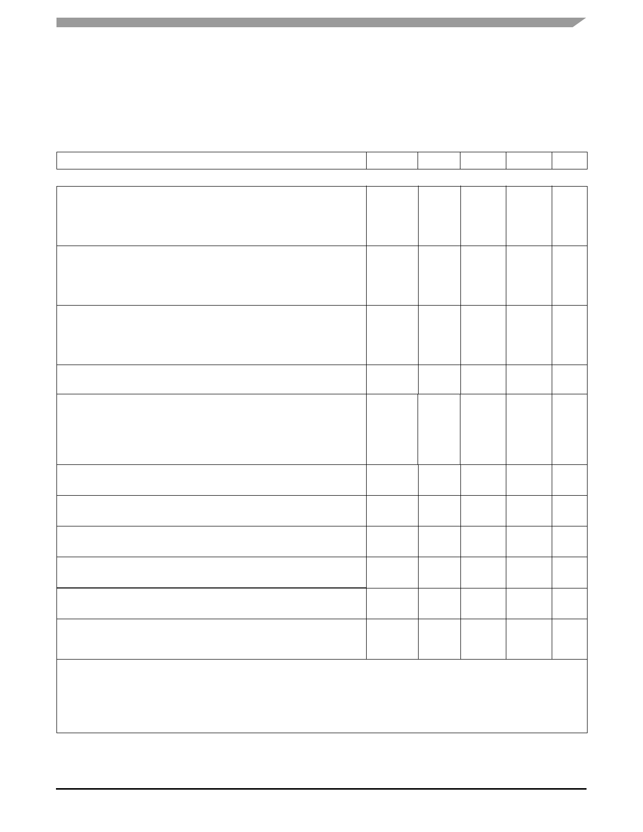
ELECTRICAL CHARACTERISTICS
DYNAMIC ELECTRICAL CHARACTERISTICS
DYNAMIC ELECTRICAL CHARACTERISTICS
Table 4. Dynamic Electrical Characteristics
Unless specified otherwise: 8.0 V VPWR 36 V, 3.0 V VDD 5.5 V, -40 C TA 125 C, GND = 0 V. Typical values are
average values evaluated under nominal conditions TA = 25 °C,VPWR = 28 V & VDD = 5.0 V, unless specified otherwise.
Parameter
Symbol
Min
Typ
Max
Unit
OUTPUT VOLTAGE SWITCHING CHARACTERISTICS
Rising and falling edge medium slew rate (SR[1:0] = 00)(28)
VPWR = 16 V
VPWR = 28 V
VPWR = 36 V
Rising edge low slew rate (SR[1:0] = 01)(28)
VPWR = 16 V
VPWR = 28 V
VPWR = 36 V
Rising edge high slew rate / SR[1:0] = 10)(28)
VPWR = 16 V
VPWR = 28 V
VPWR = 36 V
SRR_00
SRF_00
0.164
–
0.28
–
0.34
–
V/s
0.65
0.79
0.90
SRR_01
V/s
SRF_01
0.081
–
0.32
0.14
–
0.395
0.17
–
0.45
SRR_10
V/s
SRF_10
0.29
–
1.30
0.55
–
1.58
0.68
–
1.80
Rising/Falling edge slew rate matching per channel
16 V < VPWR < 36 V
Edge slew rate difference from one channel to the other in parallel mode(28)
16 V < VPWR < 36 V
SR[1:0] = 00
SR[1:0] = 01
SR[1:0] = 10
Output Turn-ON and Turn-OFF Delays (medium slew rate: SR[1:0] = 00)(29)
16 V < VPWR < 36 V
Output Turn-ON and Turn-OFF Delays (low slew rate / SR[1:0] = 01)(29)
16 V < VPWR < 36 V
Output Turn-ON and Turn-OFF Delays (high slew rate / SR[1:0] = 10)(29)
16 V < VPWR < 36 V
SRR/SRF
0.65
–
1.35
SR
V/s
-0.12
0.0
+0.12
-0.06
0.0
+0.06
-0.2
0.0
+0.2
t DLY_00
s
30
-
160
t DLY_01
s
50
-
300
t DLY_10
15
-
s
80
Turn-ON and Turn-OFF Delay time matching per channel (t DLY(ON) - t DLY(OFF))
t RF_00
f PWM = 400 Hz, 16 V < VPWR < 36 V, duty cycle on IN[x] = 50 %, SR[1:0] = 00
-25
0.0
s
25
Turn-ON and Turn-OFF Delay time matching per channel (t DLY(ON) - t DLY(OFF))
t RF_01
f PWM = 200 Hz, 16 V < VPWR < 36 V, duty cycle on IN[x] = 50 %, SR[1:0] = 01
-90
0.0
s
90
Turn-ON and Turn-OFF Delay time matching per channel (t DLY(ON) - t DLY(OFF))
t RF_10
f PWM = 1.0 kHz, 16 V < VPWR < 36 V, duty cycle on IN[x] = 50 %,
-13
0.0
SR[1:0] = 10
s
13
Notes
28. Rising and Falling edge slew rates specified for a 20% to 80% voltage variation on a 10.0 resistive load (see Figure 4).
29. Turn-on delay time measured as delay between a rising edge of the channel control signal (IN[0:1] = 1) and the associated rising edge
of the output voltage up to: VHS[0:1] = VPWR / 2 (where RL = 5.0). Turn-OFF delay time is measured as time between a falling edge of
the channel control signal (IN[0:1] = 0) and the associated falling edge of the output voltage up to the instant at which: VHS[0:1] = VPWR /
2 (RL = 10.0 )
Analog Integrated Circuit Device Data
Freescale Semiconductor
06XSD200
15
Share Link: 