MAX4416EUA 데이터 시트보기 (PDF) - Maxim Integrated
부품명
상세내역
제조사
MAX4416EUA
Maxim Integrated
MAX4416EUA Datasheet PDF : 22 Pages
| |||
Low-Power, +3V/+5V, 400MHz Single-Supply
Op Amps with Rail-to-Rail Outputs
MAX4414
MAX4415
1, 5, 8
3
—
—
—
—
2
—
—
—
—
4
6
—
—
—
—
7
PIN
MAX4416
MAX4417
—
—
3
5
—
—
—
2
6
—
—
4
—
1
7
—
—
8
MAX4418
MAX4419
—
—
3
5
10
12
—
2
6
9
13
11
—
1
7
8
14
4
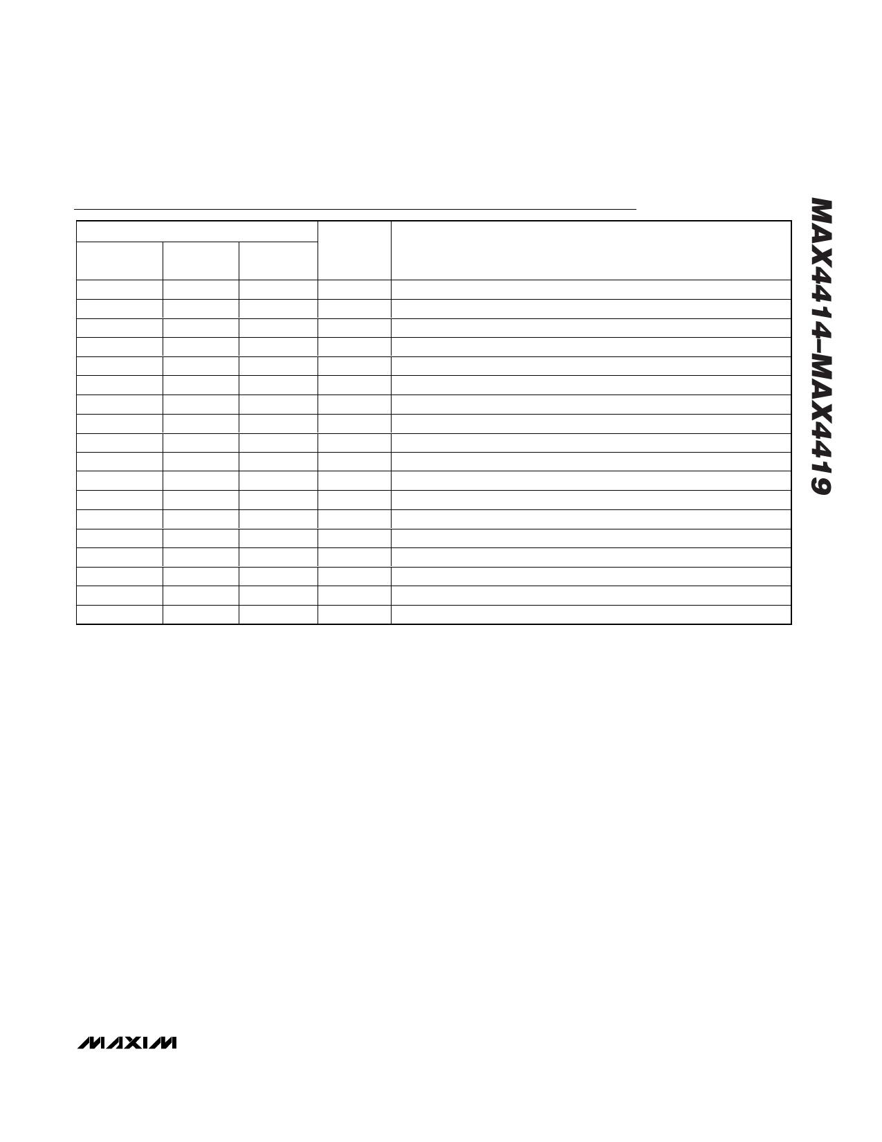
Pin Description
NAME
FUNCTION
N.C.
IN+
INA+
INB+
INC+
IND+
IN-
INA-
INB-
INC-
IND-
VEE
OUT
OUTA
OUTB
OUTC
OUTD
VCC
No Connection. Not internally connected.
Amplifier Noninverting Input
Amplifier A Noninverting Input
Amplifier B Noninverting Input
Amplifier C Noninverting Input
Amplifier D Noninverting Input
Amplifier Inverting Input
Amplifier A Inverting Input
Amplifier B Inverting Input
Amplifier C Inverting Input
Amplifier D Inverting Input
Negative Power Supply
Amplifier Output
Amplifier A Output
Amplifier B Output
Amplifier C Output
Amplifier D Output
Positive Power Supply
_______________Detailed Description
The MAX4414–MAX4419 single-supply, rail-to-rail, volt-
age-feedback amplifiers achieve high slew rates and
bandwidths, while consuming only 1.6mA of supply
current per amplifier. Excellent harmonic distortion and
differential gain/phase performance make these ampli-
fiers an ideal choice for a wide variety of video and RF
signal-processing applications.
Internal feedback around the output stage ensures low
open-loop output impedance, reducing gain sensitivity
to load variations. This feedback also produces
demand-driven current bias to the output transistors.
Rail-to-Rail Outputs, Ground-Sensing Input
The MAX4414–MAX4419 input common-mode range
extends from (VEE - 0.1V) to (VCC - 1.5V) with excellent
common-mode rejection. Beyond this range, the ampli-
fier output is a nonlinear function of the input, but does
not undergo phase reversal or latchup.
The output swings to within 105mV of either power-sup-
ply rail with a 1kΩ load. Input ground sensing and rail-
to-rail output substantially increase the dynamic range.
With a symmetric input in a single +5V application, the
input can swing 3.6Vp-p, and the output can swing
4.6Vp-p with minimal distortion.
Output Capacitive Loading and Stability
The MAX4414–MAX4419 are optimized for AC perfor-
mance. They are not designed to drive highly reactive
loads. Such loads decrease phase margin and may
produce excessive ringing and oscillation. The use of
an isolation resistor eliminates this problem (Figure 1).
Figure 2 is a graph of the Optimal Isolation Resistor
(RISO) vs. Capacitive Load.
The Small-Signal Gain vs. Frequency with Capacitive
Load and No Isolation Resistor graph in the Typical
Operating Characteristics shows how a capacitive load
causes excessive peaking of the amplifier’s frequency
response if the capacitor is not isolated from the ampli-
fier by a resistor. A small isolation resistor (usually 20Ω
to 30Ω) placed before the reactive load prevents ring-
ing and oscillation. At higher capacitive loads, AC per-
formance is controlled by the interaction of the load
capacitance and the isolation resistor. The Small-Signal
Gain vs. Frequency with Capacitive Load and 22Ω
Isolation Resistor graph shows the effect of a 22Ω isola-
tion resistor on closed-loop response.
______________________________________________________________________________________ 15
Share Link: 