MAX1421 데이터 시트보기 (PDF) - Maxim Integrated
부품명
상세내역
제조사
MAX1421 Datasheet PDF : 17 Pages
| |||
12-Bit, 40Msps, 3.3V, Low-Power ADC
with Internal Reference
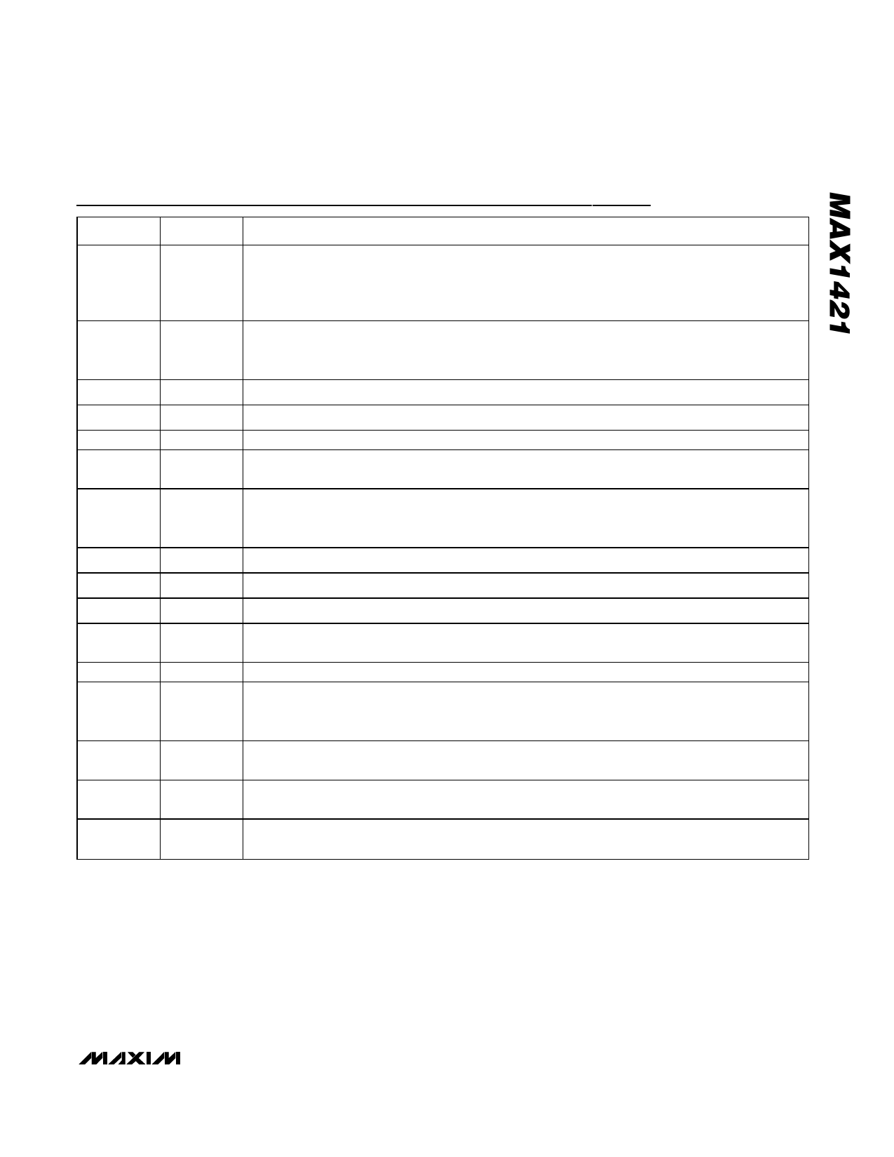
PIN
1, 4, 5, 8,
9, 12, 13,
16, 19, 41,
48
2, 3, 10,
11, 14, 15,
20, 42, 47
6
7
17
18
21, 31, 32,
22, 29, 30
23–28
33–38
39
40
43
44
45
46
NAME
FUNCTION
Pin Description
AGND
Analog Ground. Connect all return paths for analog signals to AGND.
AVDD
INP
INN
CLK
CLK
DVDD
DGND
D0–D5
D6–D11
OE
PD
REFIN
REFP
REFN
CML
Analog Supply Voltage. For optimum performance bypass each pin to the closest AGND with a
parallel combination of a 0.1µF and a 1nF capacitor. Connect a single 10µF and 1µF capacitor
combination between AVDD and AGND.
Positive Analog Signal Input
Negative Analog Signal Input
Clock Frequency Input. Clock frequency input ranges from 100kHz to 40MHz.
Complementary Clock Frequency Input. This input is used for differential clock inputs. If the ADC is
driven with a single-ended clock, bypass CLK with a 0.1µF capacitor to AGND.
Digital Supply Voltage. For optimum performance bypass each pin to the closest DGND with a
parallel combination of a 0.1µF and a 1nF capacitor. Connect a single 10µF and 1µF capacitor
combination between DVDD and DGND.
Digital Ground
Digital Data Outputs. Data bits D0 through D5, where D0 represents the LSB.
Digital Data Outputs. D6 through D11, where D11 represents the MSB.
Output Enable Input. A logic “1” on OE places the outputs D0–D11 into a high-impedance state. A
logic “0” allows for the data bits to be read from the outputs.
Shutdown Input. A logic “1” on PD places the ADC into shutdown mode.
External Reference Input. Bypass to AGND with a capacitor combination of 0.22µF in parallel with
1nF. REFIN can be biased externally to adjust reference levels and calibrate full-scale errors. To
disable the internal reference, connect REFIN to AGND.
Positive Reference I/O. Bypass to AGND with a capacitor combination of 0.22µF in parallel with 1nF.
With the internal reference disabled (REFIN = AGND), REFP should be biased to VCML + VDIFF / 2.
Negative Reference I/O. Bypass to AGND with a capacitor combination of 0.22µF in parallel with 1nF.
With the internal reference disabled (REFIN = AGND), REFN should be biased to VCML - VDIFF / 2.
Common-Mode Level Input. Bypass to AGND with a capacitor combination of 0.22µF in parallel
with 1nF. With the internal reference disabled (REFIN = AGND).
_______________________________________________________________________________________ 9
Share Link: 