LTC6103I 데이터 시트보기 (PDF) - Linear Technology
부품명
상세내역
제조사
LTC6103I Datasheet PDF : 16 Pages
| |||
LTC6103
APPLICATIONS INFORMATION
will give a lowpass response. This will reduce unwanted
noise from the output, and may also be useful as a charge
reservoir to keep the output steady while driving a switch-
ing circuit such as a mux or ADC. This output capacitor
in parallel with an output resistor will create a pole in the
output response at:
f–3dB
=
2
•
π
1
• ROUT
•
COUT
Useful Equations
Input Voltage: VSENSE = ISENSE • RSENSE
Voltage Gain: VOUT = ROUT
VSENSE RIN
Current Gain: IOUT = RSENSE
ISENSE RIN
Transconductance: IOUT = 1
VSENSE RIN
Transimpedance:
VOUT
ISENSE
= RSENSE
• ROUT
RIN
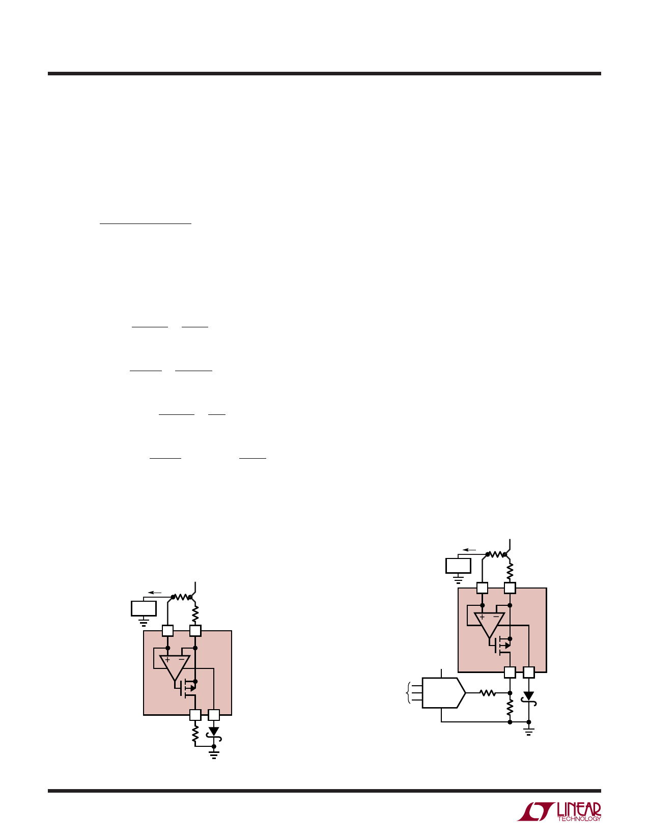
Reverse Supply Protection
Some applications may be tested with reverse-polarity
supplies due to an expectation of this type of fault during
operation. The LTC6103 is not protected internally from
V+
ILOAD RSENSE
LOAD
RIN
+IN –IN
VS
1/2
LTC6103
OUT
V–
external reversal of supply polarity. To prevent damage
that may occur during this condition, a Schottky diode
should be added in series with V– (Figure 5). This will
limit the reverse current through the LTC6103. Note that
this diode will limit the low voltage performance of the
LTC6103 by effectively reducing the supply voltage to the
part by VD.
In addition, if the output of the LTC6103 is wired to a
device that will effectively short it to high voltage (such as
through an ESD protection clamp) during a reverse sup-
ply condition, the LTC6103’s output should be connected
through a resistor or Schottky diode (Figure 6).
Response Time
The LTC6103 is designed to exhibit fast response to inputs
for the purpose of circuit protection or signal transmis-
sion. This response time will be affected by the external
circuit in two ways, delay and speed. If the output current
is very low and an input transient occurs, there may be an
increased delay before the output voltage begins changing.
This can be improved by increasing the minimum output
current, either by increasing RSENSE or decreasing RIN. The
effect of increased output current is illustrated in the step
response curves in the Typical Performance Characteristics
of this data sheet. Note that the curves are labeled with
respect to the initial output currents.
V+
ILOAD RSENSE
LOAD
8
+IN
RIN
7
–IN
TO mP
VS
1/2
LTC6103
OUT
1
R3
ADC
ROUT
V–
4
D1
ROUT
D1
6103 F06
6103 F05
Figure 5. Schottky Prevents Damage During Supply Reversal
12
Figure 6. Additional Resistor, R3, Protects
Output During Supply Reversal
6103f
Share Link: 