LTC3417AEFE-2-PBF 데이터 시트보기 (PDF) - Linear Technology
부품명
상세내역
제조사
LTC3417AEFE-2-PBF Datasheet PDF : 20 Pages
| |||
LTC3417A-2
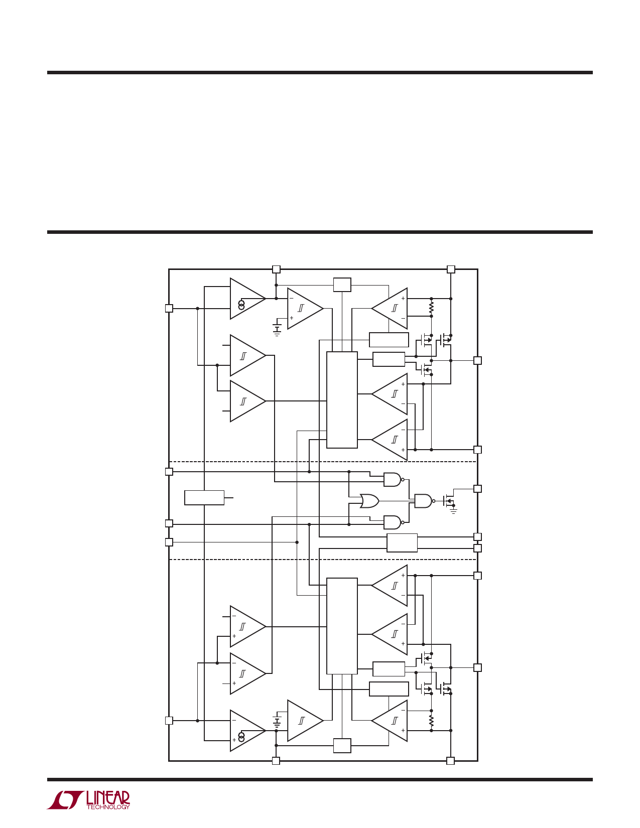
PIN FUNCTIONS ( DFN/ TSSOP)
VIN, the 1.5A regulator and the 1A regulator are in phase.
When PHASE is at 0V, the 1.5A regulator and the 1A
regulator are switching 180 degrees out-of-phase. Do
not float this pin.
SW1 ( Pi n 15/ Pi n 18) :Switch Node Connection to the
Inductor for the 1.5A Regulator. This pin swings from
VIN1 to PGND1.
PGND1 ( Pi n 16/ Pi n 19)G: round for SW1 N-Channel Driver.
PGND2, GNDD( Pi ns 1, 10, 11, 20)T:SSOP Package Only.
Ground for SW2 N-channel driver and digital ground for
circuit.
Exposed Pad ( Pi n 17/ Pi n 21)P:GND2, GNDD. Ground for
SW2 N-channel driver and digital ground for circuit. The
Exposed Pad must be soldered to PCB ground.
FUNCTIONAL DIAGRAM
1.5A REGULATOR
+
VFB1
–
0.752V +
–
+
0.848V –
ITH1
–
+
VB
ITH
LIMIT
SLOPE
COMPENSATION
ANTI-SHOOT-
THROUGH
LOGIC
VIN1
SW1
RUN1
VOLTAGE
REFERENCE
VIN2
RUN2
SYNC/MODE
PGND1
PGOOD
OSCILLATOR
PHASE
FREQ
PGND2
–
0.848V
+
–
+
0.752V
VFB2
–
+
1A REGULATOR
+
VB
–
ITH2
LOGIC
ANTI-SHOOT-
THROUGH
SLOPE
COMPENSATION
ITH
LIMIT
SW2
VIN2
3417A-2 BD
3417a2fa
7
Share Link: 